Electron emission device, electron emission type backlight unit including electron emission device, and method of fabricating electron emission device

a technology of electron emission and backlight unit, which is applied in the manufacture of electric discharge tubes/lamps, discharge tubes luminescnet screens, instruments, etc., can solve the problems of difficult to regularly emit electrons, hot spots or arc discharges,

Inactive Publication Date: 2008-03-13
SAMSUNG SDI CO LTD
View PDF4 Cites 1 Cited by
  • Summary
  • Abstract
  • Description
  • Claims
  • Application Information

AI Technical Summary

Benefits of technology

[0016] Aspects of the present invention provide an electron emission device that regularly emits electrons. Aspects of the present invention also provide an electron emission type backlight unit including the electron

Problems solved by technology

In particular, hot spots or arc discharge may occur because of high voltage app

Method used


Image

  • Electron emission device, electron emission type backlight unit including electron emission device, and method of fabricating electron emission device
  • Electron emission device, electron emission type backlight unit including electron emission device, and method of fabricating electron emission device
  • Electron emission device, electron emission type backlight unit including electron emission device, and method of fabricating electron emission device

Examples


Embodiment Construction

[0040] Reference will now be made in detail to the present embodiments of the present invention, examples of which are illustrated in the accompanying drawings, wherein like reference numerals refer to the like elements throughout. The embodiments are described below in order to explain the present invention by referring to the figures. Herein, when a layer is said to be “disposed on” another layer or a substrate, the phrase refers to a layer that may be directly formed on the other layer, or that a third layer may be disposed therebetween. In addition, the thickness of layers and regions may be exaggerated for clarity.

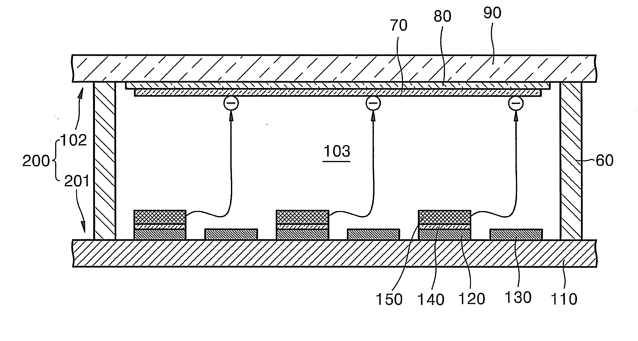
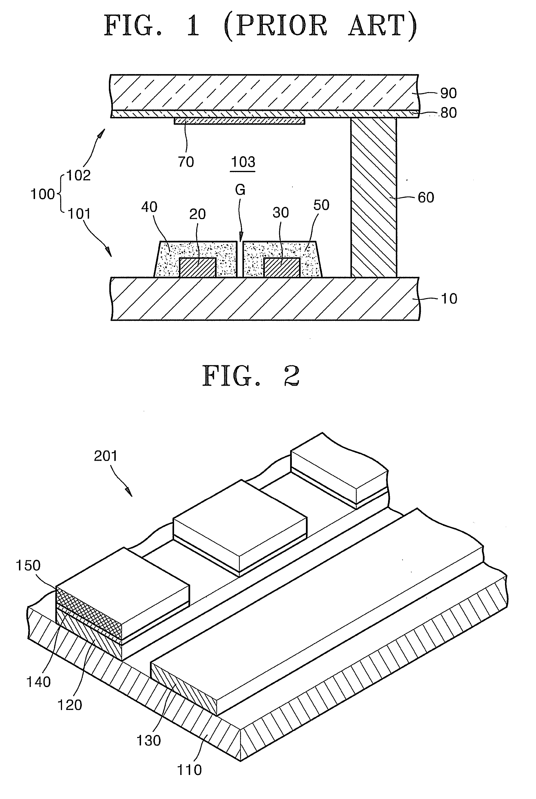
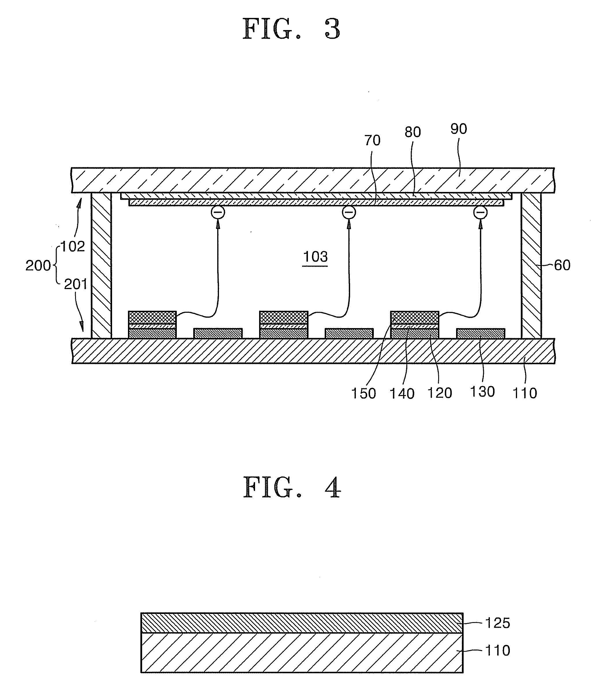
[0041]FIG. 2 is a partial perspective view illustrating an electron emission device 201 according to aspects of the present invention. Referring to FIG. 2, the electron emission device 201 includes a base substrate 110, a plurality of first electrodes 120, a plurality of second electrodes 130 and a plurality of electron emission layers 150. The base substrate 110 is ...


PUM


Abstract

An electron emission device to regularly emit electrons and a method of manufacturing the same. Also, an electron emission type backlight unit including the electron emission device in which a high voltage can be applied to an anode and required brightness can be obtained. In addition, the electron emission device can be manufactured using a simplified manufacturing process. The electron emission device includes a first electrode, a second electrode formed opposite the first electrode, and an electron emission layer which is electrically connected to one or each of the first and second electrodes and comprising carbide-derived carbon. The electron emission device may be a display device to form static or dynamic images.

Description

CROSS-REFERENCE TO RELATED PATENT APPLICATIONS [0001] This application claims the benefit of Korean Application No. 2006-87423, filed Sep. 11, 2006, in the Korean Intellectual Property Office, the disclosure of which is incorporated herein in its entirety by reference. BACKGROUND OF THE INVENTION [0002] 1. Field of the Invention [0003] Aspects of the present invention relate to an electron emission device, an electron emission type backlight unit, and a method of fabricating the electron emission device, and more particularly, to an electron emission device that regularly emits electrons, an electron emission type backlight unit including the electron emission device, and a method of fabricating the electron emission device. [0004] 2. Description of the Related Art [0005] Generally, electron emission devices use a hot cathode or a cold cathode as an electron emission source. Examples of electron emission devices having a cold cathode include a field-emitter array (FEA) type, a surfa...

Claims


Application Information

Patent Timeline
IPC IPC(8): H01J1/62H01J1/14H01J9/00
CPCH01J1/30H01J2201/319H01J63/02H01J9/022G02F1/1336
Inventor KIM, YOON-JINKIM, JAE-MYUNGMOON, HEE-SUNG
Owner SAMSUNG SDI CO LTD
Why Eureka
Try Eureka