Electronic circuit, optoelectronic device, method for driving optoelectronic device, and electronic apparatus

a technology of optoelectronic devices and electronic circuits, applied in static indicating devices, solid-state devices, instruments, etc., can solve problems such as difficult compensation, increased low-scale data writing speed, and insufficient data writing

Active Publication Date: 2008-03-20
BOE TECH GRP CO LTD
View PDF13 Cites 6 Cited by
  • Summary
  • Abstract
  • Description
  • Claims
  • Application Information

AI Technical Summary

Benefits of technology

[0012] If a current signal is used as the first signal to drive an electronic element by using the above-described electronic circuit, the accuracy of driving the electronic element increases. Further, if a voltage signal is used as the second signal, the speed of driving the electronic element increases.
[0035] Accordingly, it becomes possible to set the timing of transmitting the first signal and the timing of transmitting the second signal by controlling the conduction state of the second transistor.

Problems solved by technology

For low gray-scale display, data is often inadequately written because of capacitance of wiring such as a data line or the like.
It is particularly difficult to compensate for the characteristic variations in the active elements and increase the speed of writing low gray-scale data.
In particular, according to a driving method to transmit a data-current or a current signal as a data signal to compensate for the characteristic variations of the active elements, inadequate data writing tends to be significant.

Method used


Image

  • Electronic circuit, optoelectronic device, method for driving optoelectronic device, and electronic apparatus
  • Electronic circuit, optoelectronic device, method for driving optoelectronic device, and electronic apparatus
  • Electronic circuit, optoelectronic device, method for driving optoelectronic device, and electronic apparatus

Examples


first exemplary embodiment

[0074] A first exemplary embodiment of the present invention will be described with reference to FIGS. 1 to 4.

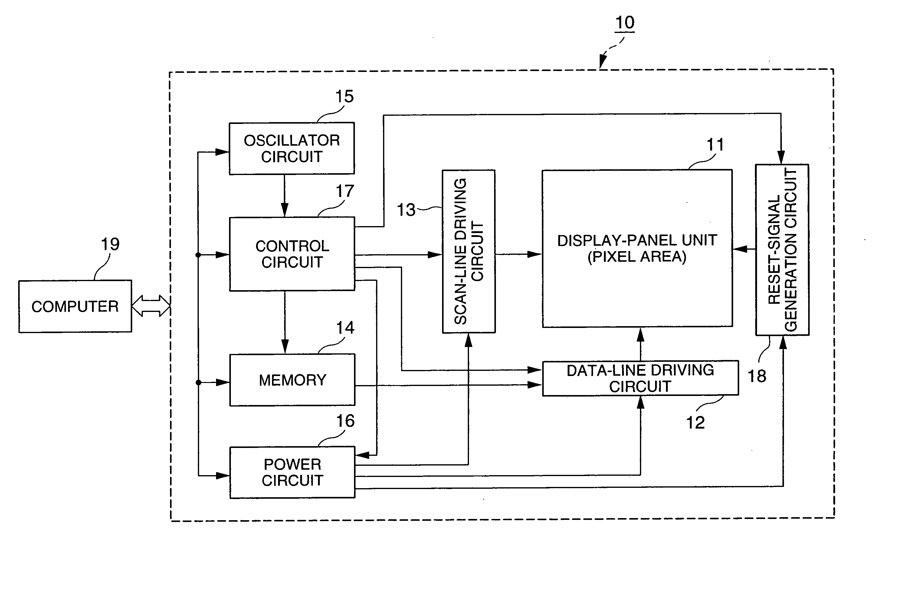
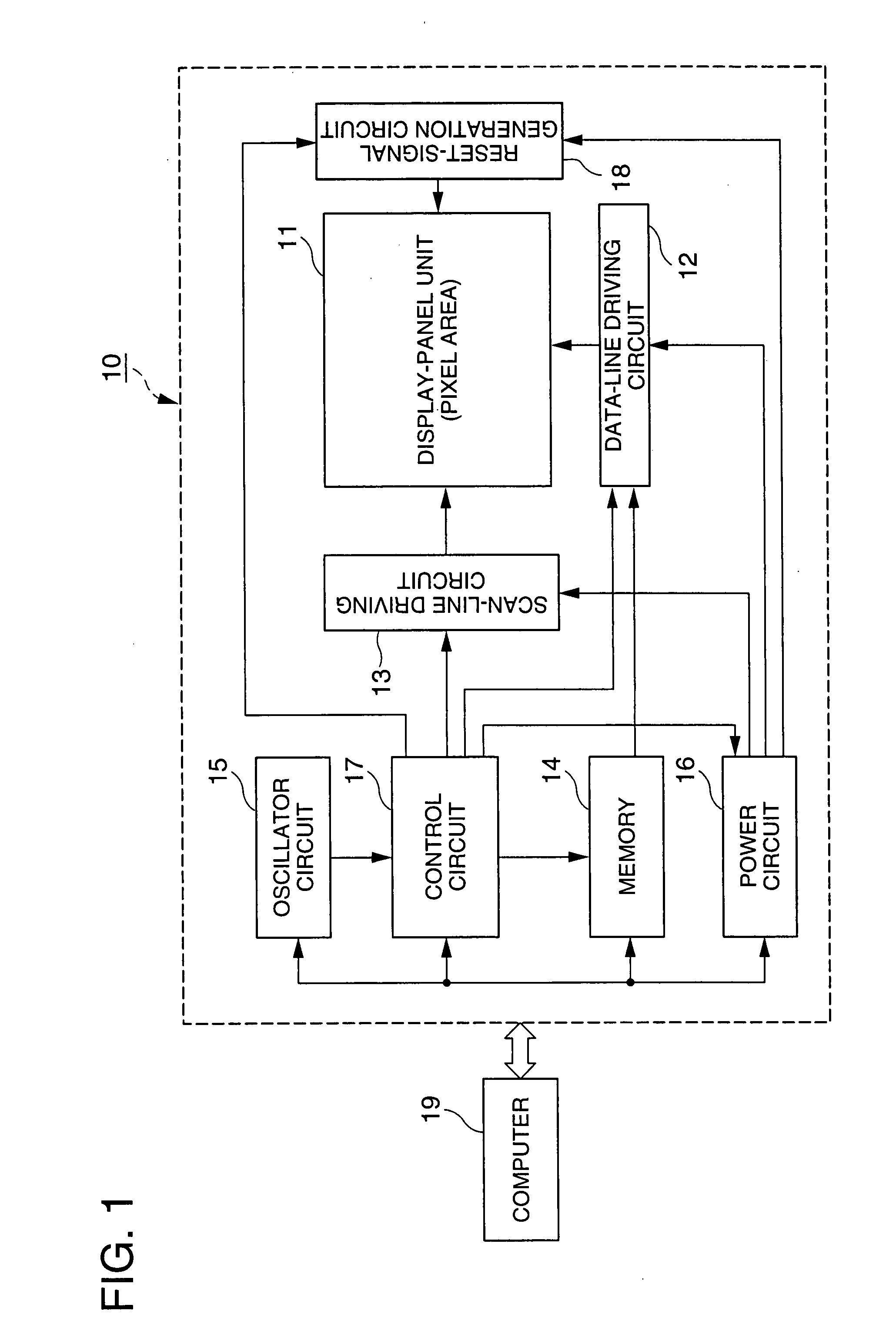
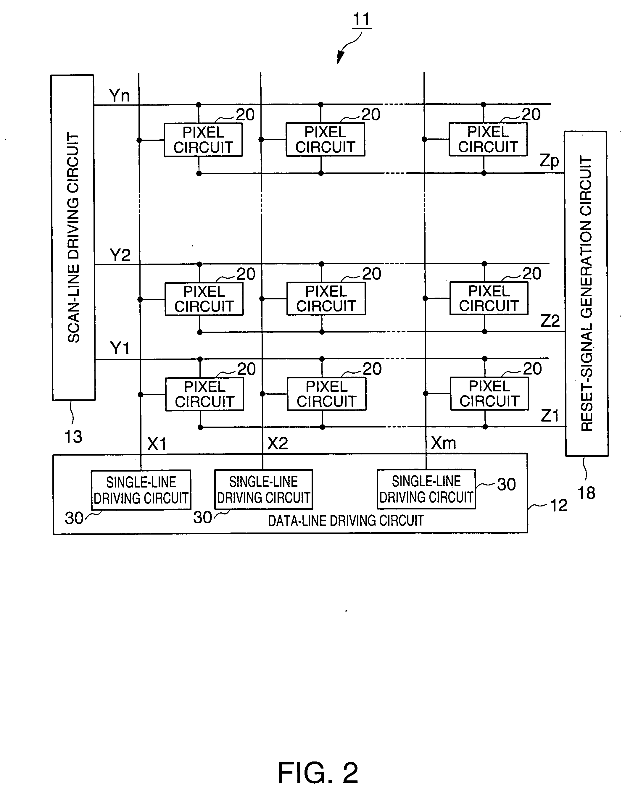
[0075]FIG. 1 is a block diagram illustrating the circuit configuration of an organic EL device 10 functioning as an electronic device. FIG. 2 is a block diagram illustrating the internal circuit configuration of a display-panel unit and a data-line driving circuit. FIG. 3 is a circuit diagram illustrating the internal configuration of a pixel circuit and electronic circuits relating to the pixel circuit.

[0076] In FIG. 1, the organic EL device 10 functioning as the electronic device comprises a display-panel unit 11, a data-line driving circuit 12, a scan-line driving circuit 13, a memory 14, an oscillator circuit 15, a power circuit 16, a control circuit 17, and a reset-signal generation circuit 18.

[0077] The elements 11 to 18 of the organic EL device 10 may be formed as electronic parts independent of one another. For example, the elements 12 to 18 may be formed as a sem...

second exemplary embodiment

[0113] A second exemplary embodiment of the present invention will now be described with reference to FIG. 5.

[0114] In this exemplary embodiment, the data line to transmit a data signal is also used as a signal line to transmit a reset signal. In contrast to the first exemplary embodiment, a reset-voltage generation circuit 41b is provided in the data-line driving circuit 12, in place of the reset-signal generation circuit 18.

[0115]FIG. 5 illustrates the pixel circuit 20 provided at the intersection of the first data line X1 and the first scan line Y1. In this exemplary embodiment, each of the scan lines Y1 to Yn includes one scan line corresponding to the second scan line Vb, in contrast to the scan lines Y1 to Yn of the first exemplary embodiment.

[0116] The pixel circuit 20 includes a driving transistor Q20 as a first transistor, first and second switching transistors Q21 and Q22, a holding capacitor C1 as a holding element, and a compensation transistor Q23.

[0117] Each of the...


PUM

PropertyMeasurementUnit
currentaaaaaaaaaa
voltageaaaaaaaaaa
driving voltageaaaaaaaaaa

Abstract

An electronic circuit, an electronic device, and an electronic apparatus are provided that are capable of display with good quality and reducing operation delay, and a method to drive the electronic circuit. First and second switching transistors are turned on and an operation voltage Vdx and a data-current Idata are transmitted to a holding capacitor. The conduction state of a driving transistor is set according to an electrical-charge amount corresponding to the data-current Idata held in the holding capacitor and a current that passes the driving transistor is transmitted to an organic EL element. Then, a first switch is turned off, a second switch and the second switching transistor are turned on, and a reset voltage Vr is transmitted to the holding capacitor, whereby the driving transistor is turned off and the organic EL element stops emitting light.

Description

[0001] This is a Continuation of application Ser. No. 10 / 444,420 filed May 27, 2003. The disclosure of the prior application is hereby incorporated by reference herein in its entirety.BACKGROUND OF THE INVENTION [0002] 1. Field of Invention [0003] The present invention relates to an electronic circuit, an optoelectronic device, a method to drive the optoelectronic device, and an electronic apparatus. [0004] 2. Description of Related Art [0005] Recently, optoelectronic devices with high definition and a large screen have been in demand. The optoelectronic devices have a plurality of optoelectronic elements and are widely used as a display device. Therefore, dependency on active-matrix-drive optoelectronic devices having pixel circuits to drive each of the plurality of optoelectronic elements has been becoming greater than that on passive-drive optoelectronic devices. However, the plurality of optoelectronic elements need to be controlled with precision to obtain increased high defini...

Claims


Application Information

Patent Timeline
Patent Type & Authority Applications(United States)
IPC IPC(8): G06F3/038G02F1/133G09G3/20G09G3/30G09G3/32G09G3/36H01L51/50
CPCG09G3/3241G09G3/325G09G2300/043G09G2320/0223G09G2310/0251G09G2310/0262G09G2300/0842G09G3/20
Inventor MIYAZAWA, TAKASHI
Owner BOE TECH GRP CO LTD
Why Eureka
Try Eureka