Solid-state image sensing device with a change-over switch

a technology of solid-state image and switch, which is applied in the direction of radiation controlled devices, optical radiation measurement, pulse technique, etc., can solve the problems of deteriorated pixel drive accuracy, increased voltage drop and charging/discharging time, and inability to sharply raise or drop the pixel drive signal, etc., to achieve the effect of improving the pixel drive accuracy, reducing resistance and parasitic capacitance of the wiring, and improving the accuracy of the pixel driv

Inactive Publication Date: 2015-04-28
HONDA MOTOR CO LTD
View PDF47 Cites 1 Cited by
  • Summary
  • Abstract
  • Description
  • Claims
  • Application Information

AI Technical Summary

Benefits of technology

[0008]Accordingly, in view of the above conventional problem, an object of the present invention is to provide a solid-state image sensing device capable of performing the high-speed global shutter operation without the pixel drive accuracy deterioration.
[0017]In the present invention, the solid-state image sensing device comprises the unit pixel containing the photoelectric conversion element for detecting the light to generate the photoelectrons and the at least one electrode for forming the MOS diode structure, the first contact point connected to the first voltage supply for supplying the first voltage to the electrode, the second contact point connected to the second voltage supply for supplying the second voltage higher than the first voltage to the electrode, the first capacitor disposed between the first and second contact points, the change-over switch, which is connected to one of the first and second contact points to selectively switch the voltage applied to the electrode to the first or second voltage, and the pixel drive circuits for driving the change-over switch, thereby alternately applying the first and second voltages to the electrode to generate, hold, transfer, reset, or discharge the photoelectrons. Therefore, the first and second voltages of pixel drive signals for driving the unit pixel can be sharply raised and dropped by the first capacitor to improve the pixel drive accuracy. Thus, the global shutter operation can be performed at high speed.
[0018]When the solid-state image sensing device further comprises the third contact point connected to the third voltage supply (for supplying the third voltage higher than the first voltage and lower than the second voltage to the electrode) and the second capacitor disposed between the first and third contact points, and the pixel drive circuits control the switch to apply the third voltage to the electrode in the processes of switching the voltage applied to the electrode from the first voltage to the second voltage and from the second voltage to the first voltage, the voltage drop of the second contact point can be reduced in the process of switching the voltage applied to the electrode from the first voltage to the second voltage to further improve the pixel drive accuracy.
[0019]When the voltage is applied to the upper side of the electrode, and the lower side is wire-connected to the first contact point inside the solid-state image sensing device and is further wire-connected to the first voltage supply, the resistance and parasitic capacitance of the wiring can be reduced and thus the time constant obtained therefrom can be reduced by minimizing the wiring. Therefore, the electrode can be rapidly charged and discharged, the pixel drive signal for driving the unit pixel can be more sharply raised, and the gate drive signal operation can be performed at high speed, to improve the pixel drive accuracy.

Problems solved by technology

However, in the technologies described in Japanese Laid-Open Patent Publication Nos. 2010-268079 and 2009-296400, the pixel drive signal cannot be sharply raised or dropped though the peak current can be reduced.
Therefore, in a high-speed global shutter operation, the pixel drive signal cannot be applied to the pixel as desired, resulting in deteriorated pixel drive accuracy.
However, the voltage drop and charging / discharging time are increased due to the electric supply line resistance and parasitic capacitance.
Particularly in a case where the process of transferring the generated photoelectrons to an electron hold unit is performed multiple times in one frame in a TOF (time-of-flight) distance sensor, when the gate electrode in the pixel is repeatedly controlled multiple times at an interval of several hundred nanoseconds, the electric charge cannot be supplied from the external power source to the gate electrode at a sufficient speed and the desired voltage cannot be applied disadvantageously.

Method used


Image

  • Solid-state image sensing device with a change-over switch
  • Solid-state image sensing device with a change-over switch
  • Solid-state image sensing device with a change-over switch

Examples


modified example 1

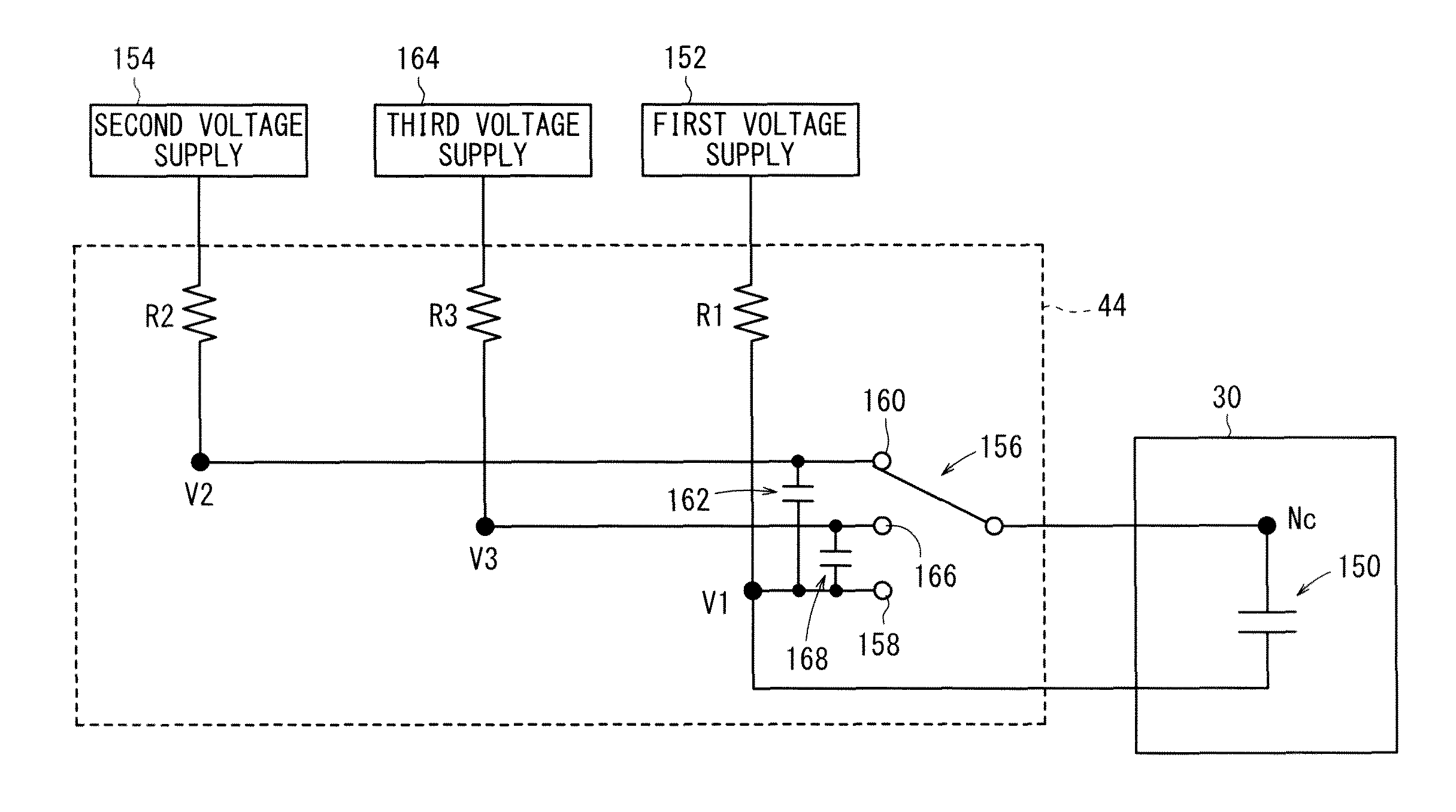
[0129]In Modified Example 1, the gate drive circuit 44 has a structure shown in FIG. 22. Thus, in Modified Example 1, the gate drive circuit 44 has a third contact point 166 connected to a third voltage supply (intermediate voltage supply) 164 for applying a third voltage to the gate of the pixel load capacitance 150 in the unit pixel 30, and further has a capacitor (second capacitor) 168 between the first contact point 158 and the third contact point 166. The change-over switch 156 acts to selectively apply the first, second, and third voltages to the gate of the pixel load capacitance 150. The third voltage is an intermediate voltage (intermediate signal voltage) higher than the first voltage and lower than the second voltage. The third voltage supply 164 is mounted in the power source 20. In FIG. 22, R3 represents a wiring resistance between the third voltage supply 164 and the third contact point 166. The same components are marked with the same numerals in FIGS. 18 and 22. The ...

modified example 2

[0137]Though the unit pixel 30 has the four light receiving devices 100 in the above embodiment, the unit pixel 30 may have only one light receiving device 100 or a plurality of light receiving devices 100 (e.g. two, three, or five light receiving devices 100). Furthermore, though the light receiving device 100 has the four photoelectron distributors 106 in the above examples, the light receiving device 100 may have only one photoelectron distributor 106 or a plurality of photoelectron distributors 106 (e.g. two, three, or five photoelectron distributors 106).

[0138]In addition, though the change-over switch 156, the first contact point 158, the second contact point 160, and a third contact point 166 are formed in the gate drive circuit 44 in the above examples, they may be formed outside the gate drive circuit 44.


PUM


Abstract

A solid-state image sensing device comprises a unit pixel containing a photoelectric conversion element for detecting a light to generate photoelectrons and at least one electrode for forming an MOS diode structure, a first contact point connected to a first voltage supply for supplying a first voltage to the electrode, a second contact point connected to a second voltage supply for supplying a second voltage higher than the first voltage to the electrode, a first capacitor disposed between the first and second contact points, a change-over switch connected to one of the first and second contact points to selectively switch a voltage applied to the electrode to the first voltage or the second voltage, and pixel drive circuits for driving the change-over switch, thereby alternately applying the first voltage and the second voltage to the electrode to generate, hold, transfer, reset, or discharge the photoelectrons.

Description

CROSS-REFERENCE TO RELATED APPLICATION[0001]This application is based upon and claims the benefit of priority from Japanese Patent Application No. 2011-081327 filed on Mar. 31, 2011, of which the contents are incorporated herein by reference.BACKGROUND OF THE INVENTION[0002]1. Field of the Invention[0003]The present invention relates to a solid-state image sensing device with improved pixel drive accuracy.[0004]2. Description of the Related Art[0005]To realize a global electronic shutter function for simultaneously performing light-receiving processes of pixels, a conventional voltage drop problem caused by a peak current has to be solved. When a voltage of a pulse pixel drive signal is applied to a gate to drive the pixel, the peak current is generated. The peak current causes the voltage drop in combination with a wiring resistance or the like. In Japanese Laid-Open Patent Publication No. 2010-268079, the peak current is reduced by delaying a light-receiving timing to prevent the ...

Claims


Application Information

Patent Timeline
Patent Type & Authority Patents(United States)
IPC IPC(8): H03K17/78H01L27/00H01L27/148H04N5/353H04N5/3745
CPCH01L27/14812H01L27/14831H04N5/353H04N5/37452H04N25/53H04N25/771
Inventor KAMIYAMA, TOMOYUKIKOREKADO, KEISUKE
Owner HONDA MOTOR CO LTD
Why Eureka
Try Eureka