Semiconductor package and semiconductor system in package using the same

a technology of semiconductor and package, applied in the field of semiconductor package, can solve the problems of low reliability and mechanical strength of conventional sip, and the space requirements of conventional package-on-package-type sip, and achieve the effect of reducing volum

Inactive Publication Date: 2008-03-27
SAMSUNG ELECTRONICS CO LTD
View PDF2 Cites 88 Cited by
  • Summary
  • Abstract
  • Description
  • Claims
  • Application Information

AI Technical Summary

Benefits of technology

[0012]Accordingly, the present invention has been made to solve the problems occurring...

Problems solved by technology

One disadvantage of the conventional package-on-package-type SIP is that the conventional package-on-package-type SIP requires much space for solder balls, which are inserted between the first and second semiconductor packages, as the present application of...

Method used


Image

  • Semiconductor package and semiconductor system in package using the same
  • Semiconductor package and semiconductor system in package using the same
  • Semiconductor package and semiconductor system in package using the same

Examples


Embodiment Construction

[0021]Hereinafter, several aspects of the present invention will be described in detail with reference to the accompanying drawings. For the purposes of clarity and simplicity, a detailed description of known functions and configurations is omitted as they may make the subject matter of the present invention unclear.

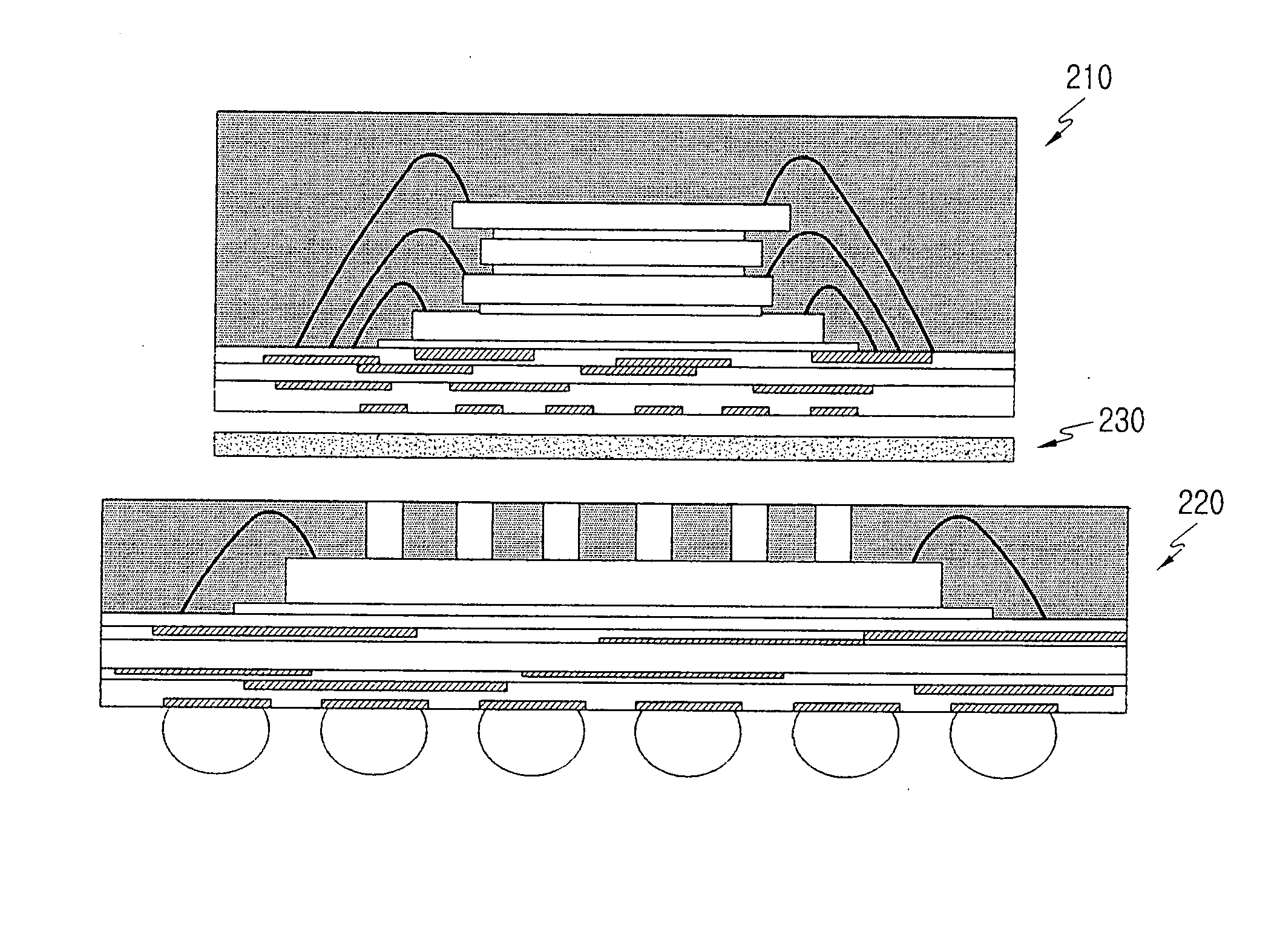
[0022]FIG. 2A is a sectional view showing a SIP according to the first aspect of the present invention, whereas FIGS. 3A to 3D are sectional views showing the manufacturing step of the SIP shown in FIG. 2A. Referring to FIGS. 2A, 2B, and 3A to 3D, a SIP 200 according to the first aspect includes first and second semiconductor packages 220 and 210. The second semiconductor package 210 is disposed on the first semiconductor package 220.

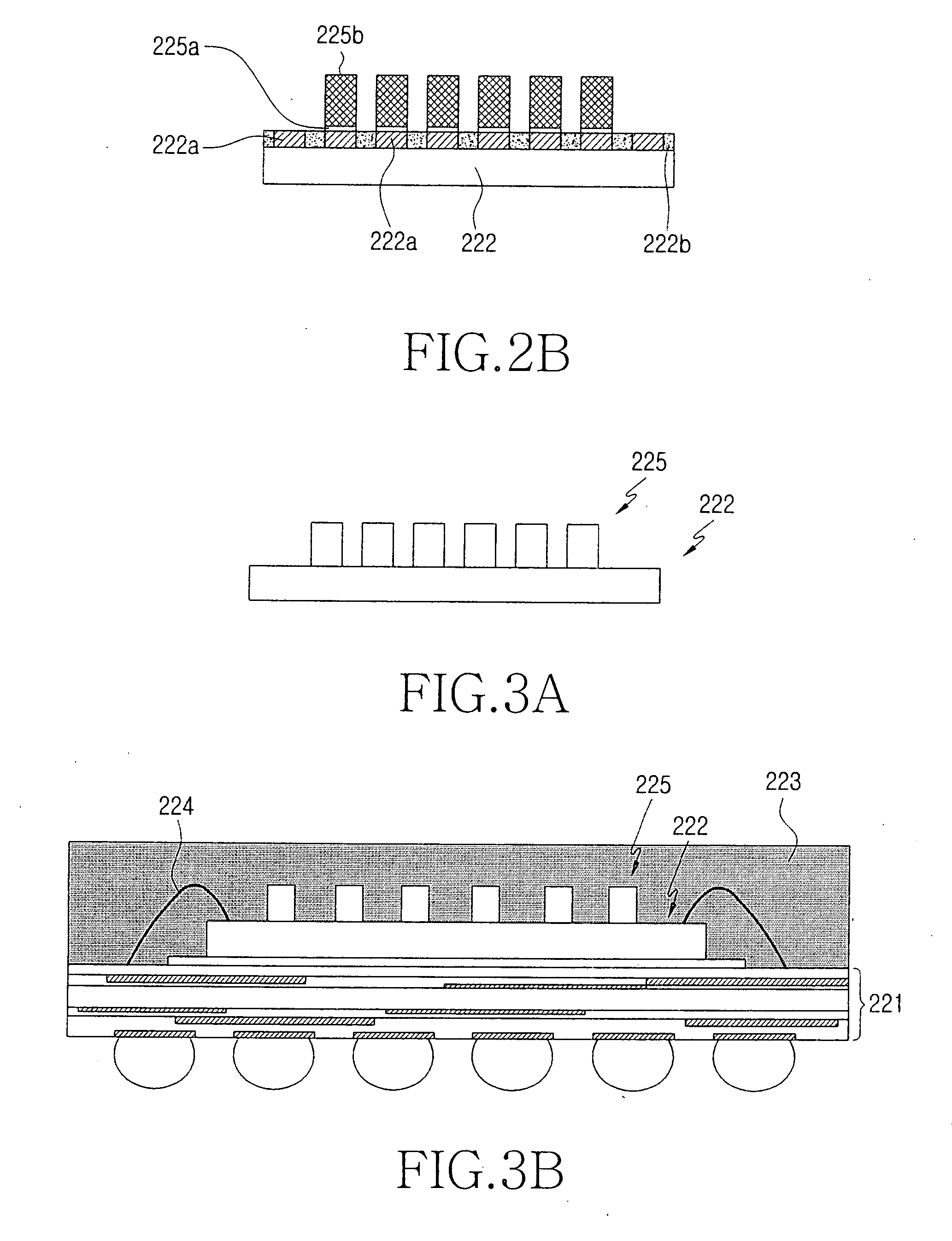
[0023]The first semiconductor package 220 includes a semiconductor die 222, on which wiring redistributions 225 are formed; a molding 223 with exposed upper surface, the molding 223 through which the wiring redistributions 225 extend; and a ...


PUM


Abstract

Disclosed are a semiconductor package and semiconductor system in package using the same. The semiconductor package includes: a printed circuit board (PCB); a semiconductor die disposed on the PCB and having conductive posts formed on an upper surface of the semiconductor die; and a molding formed on the PCB to cover the semiconductor die, wherein the conductive posts have a surface exposed out of an upper surface of the molding. The semiconductor system in package includes: a first semiconductor package having a semiconductor die on which conductive posts are formed, and a molding formed so that upper surfaces of the conductive posts are exposed; and a second semiconductor package disposed on the first semiconductor package and electrically connected to the conductive posts.

Description

CLAIM OF PRIORITY[0001]This application claims priority to an application entitled “Semiconductor Package and Semiconductor System In Package Using the Same,” filed in the Korean Intellectual Property Office on Sep. 26, 2006 and assigned Serial No. 2006-93433, the contents of which are hereby incorporated by reference.BACKGROUND OF THE INVENTION[0002]1. Field of the Invention[0003]The present invention relates to a semiconductor package that has a semiconductor die mounted thereon, and more particularly to a system in package (SIP) in which semiconductor packages are electrically connected to each other.[0004]2. Description of the Related Art[0005]A System In Package (SIP) refers to a package for modulating large scale integrated circuits such as a semiconductor die, which is applied to portable terminals which have difficulty in securing a mounting space. Recently, the SIP has been applied to various fields.[0006]The SIP may be classified into a wire bonding-type SIP, a package on ...

Claims


Application Information

Patent Timeline
IPC IPC(8): H01L23/48H01L21/02H01L23/02
CPCH01L21/56H01L23/3128H01L2924/00011H01L2224/293H01L2224/2929H01L2224/32225H01L2225/1058H01L2225/1023H01L2224/73207H01L2224/73265H01L2924/01033H01L2924/15331H01L2924/15311H01L2924/14H01L2924/01029H01L2225/06582H01L2225/06575H01L2225/0651H01L2224/83851H01L2224/83101H01L2224/48227H01L2224/48091H01L24/12H01L24/16H01L24/48H01L24/73H01L24/83H01L25/0657H01L25/105H01L2224/16H01L2224/32145H01L2924/00014H01L2924/00012H01L2224/29075H01L2924/181H01L2224/45099H01L2224/45015H01L2924/207H01L23/28H01L23/16
Inventor SEO, HO-SEONGCHO, SHI-YUNLEE, YOUNG-MINKIM, SANG-HYUN
Owner SAMSUNG ELECTRONICS CO LTD
Why Eureka
Try Eureka