
Probe based patterning of microelectronic and micromechanical devices

Inactive Publication Date: 2008-03-27
INTEL CORP
View PDF14 Cites 3 Cited by
  • Summary
  • Abstract
  • Description
  • Claims
  • Application Information

AI Technical Summary

Problems solved by technology

One obstacle to producing still smaller features is the wavelength of the light being used.
As the wavelength of the illumination light gets smaller, the lithography process becomes more difficult and more expensive.
As a result, the projection optics cannot be made using transparent lenses and the best mirrors so far developed reflect only about 70% of the light that shines on them.
This compares poorly with even poor quality visible light mirrors that reflect more than 95% of the light that shines on them.
The absorption of EUV light also produces unwanted heat and wear on any materials that may be used in an EUV photolithography process, included the materials in the mask.
The combination of the difficult EUV light and E-Beam patterning is expected to be significantly more costly than the current optical methods.
Another difficulty is the high speed desired in semiconductor manufacturing to keep costs down and volumes high.
These are expected to be very hard to make without some defects.
Direct write lithography is a serial writing approach using, for example, an E-beam and is expected to be too slow for high volume manufacturing.

Method used


Image

  • Probe based patterning of microelectronic and micromechanical devices
  • Probe based patterning of microelectronic and micromechanical devices
  • Probe based patterning of microelectronic and micromechanical devices

Examples


Embodiment Construction

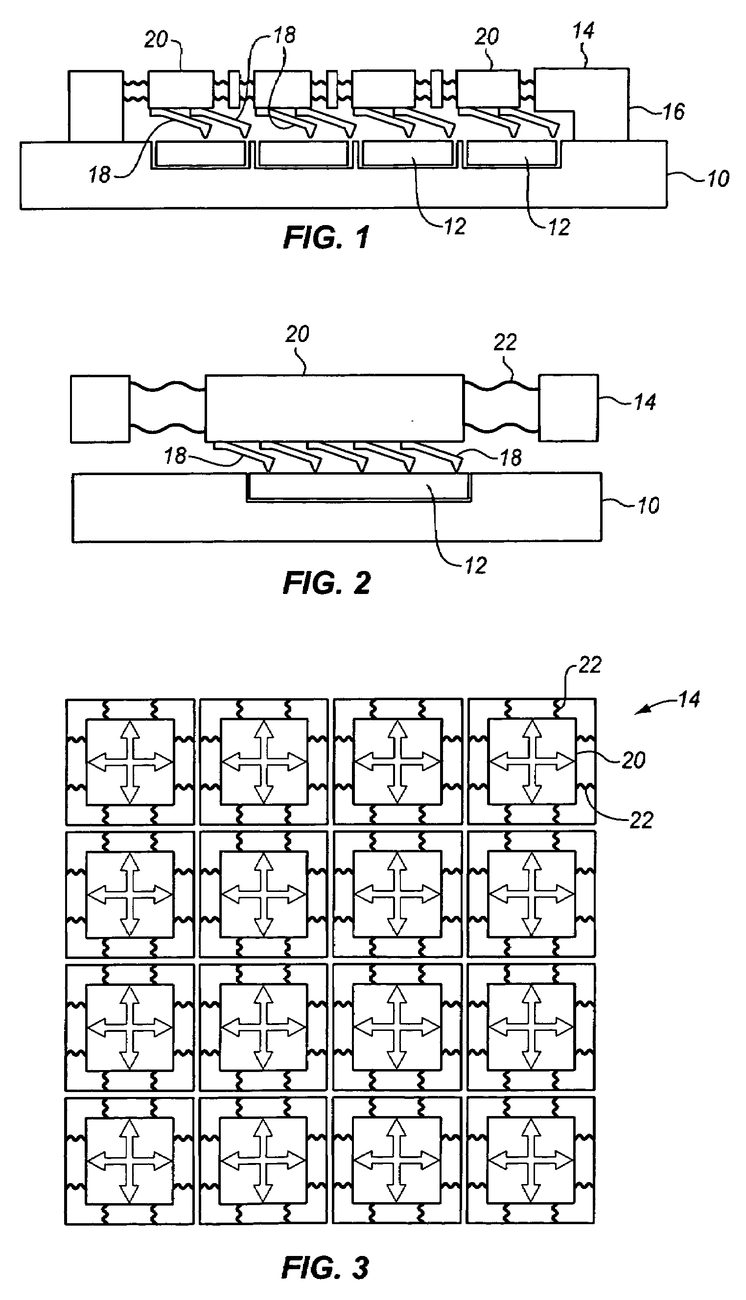
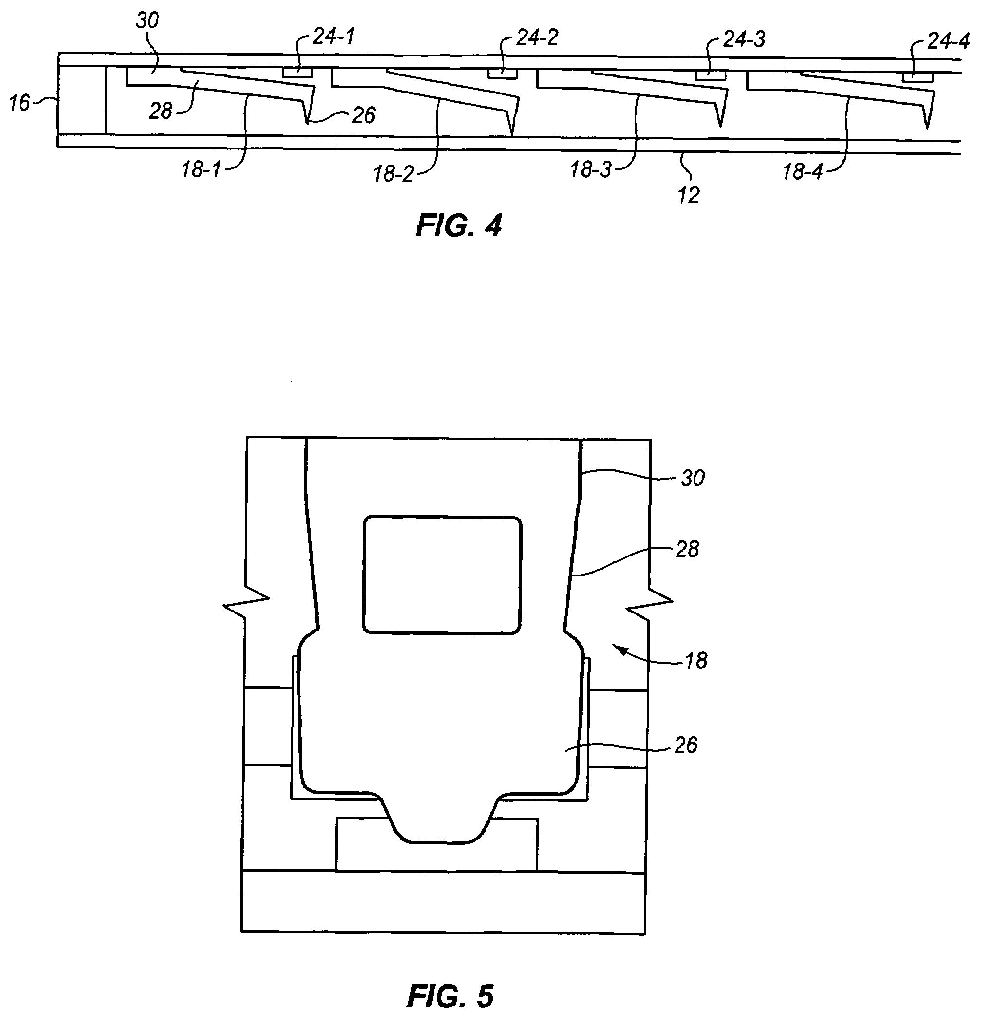
[0020]New ways to pattern substrates are described. These can be used instead of or in combination with current techniques that use electromagnetic radiation (light, X-Rays etc) or charged particle beams (E-Beam, Ion Beam etc). As described below, a sharp mechanical probe tip may be used to indent or emboss patterns directly into photoresist or any other suitable material. The probe is attached to a high precision X-Y positioning stage. Current stages can position a probe to within fractions of a nanometer. This may allow for significantly smaller features to be produced than even EUV will be able to achieve.

[0021]By forming an array of probes on an X-Y positioning stage, with each probe scanning a small area, large substrate areas may be patterned in a short amount of time. This is accomplished by taking advantage of the parallelism afforded by the many probes. Even though the scan travel of a single probe tip may be small (for example about 50 micrometers), a large area can be cov...


PUM


Abstract

Patterning of microelectronic and micromechanical devices is described using probes. In one example, a plurality of probe tips are driven into a processing layer of a substrate. The probe tips are carried by movable sleds. The sleds are moved to write patterns into the processing layer using the probes, and the processing layer is processed to form features on the substrate.

Description

BACKGROUND[0001]1. Field[0002]The present description relates to the field of patterning microelectronic and micromechanical devices, and in particular, to forming patterns using an array of probe tips to indent a photoresist or mask layer.[0003]2. Related Art[0004]To increase the number of transistors, diodes, resistors, capacitors, and other circuit elements on an integrated circuit chip, these devices are placed closer and closer together. This requires that each device be made smaller.[0005]Current manufacturing technologies use laser light with a wavelength of 193 nm for photolithography. These are referred to as Deep Ultraviolet (DUV) systems. These systems which are the workhorses of 65 nm lithography in 2006 are being continuously improved and are projected to be used to produce features as small as 20 nm. However, at this point, it is anticipated that a different technology must be applied.[0006]One obstacle to producing still smaller features is the wavelength of the light...

Claims


Application Information

Patent Timeline
IPC IPC(8): G01R31/02
CPCB81C1/00031B81C2201/0154B81C2201/0198G03F7/2049B82Y40/00G03F7/0002B82Y10/00
Inventor RAO, VALLURI
Owner INTEL CORP
Learn More