
Package for mixed signal mcu with minimal pin count

a mixed signal and pin count technology, applied in the field of packaging devices, can solve the problems of presenting difficulties, pin count beyond which the chip cannot function,

Inactive Publication Date: 2008-04-03
SILICON LAB INC
View PDF3 Cites 39 Cited by
  • Summary
  • Abstract
  • Description
  • Claims
  • Application Information

AI Technical Summary

Problems solved by technology

Of course, there is a minimal pin count beyond which the chip cannot function.
This presents some difficulty when considering that these small packages can have microprocessors disposed therein.

Method used


Image

  • Package for mixed signal mcu with minimal pin count
  • Package for mixed signal mcu with minimal pin count
  • Package for mixed signal mcu with minimal pin count

Examples


Embodiment Construction

[0020]Referring now to the drawings, wherein like reference numbers are used herein to designate like elements throughout the various views, embodiments of the present invention are illustrated and described, and other possible embodiments of the present invention are described. The figures are not necessarily drawn to scale, and in some instances the drawings have been exaggerated and / or simplified in places for illustrative purposes only. One of ordinary skill in the art will appreciate the many possible applications and variations of the present invention based on the following examples of possible embodiments of the present invention.

[0021]It will be appreciated by those skilled in the art having the benefit of this disclosure that this invention provides a low cost MCU device with a minimal pin count package, where the package cost is a smaller fraction of the total cost. It should be understood that the drawings and detailed description herein are to be regarded in an illustra...


PUM


Abstract

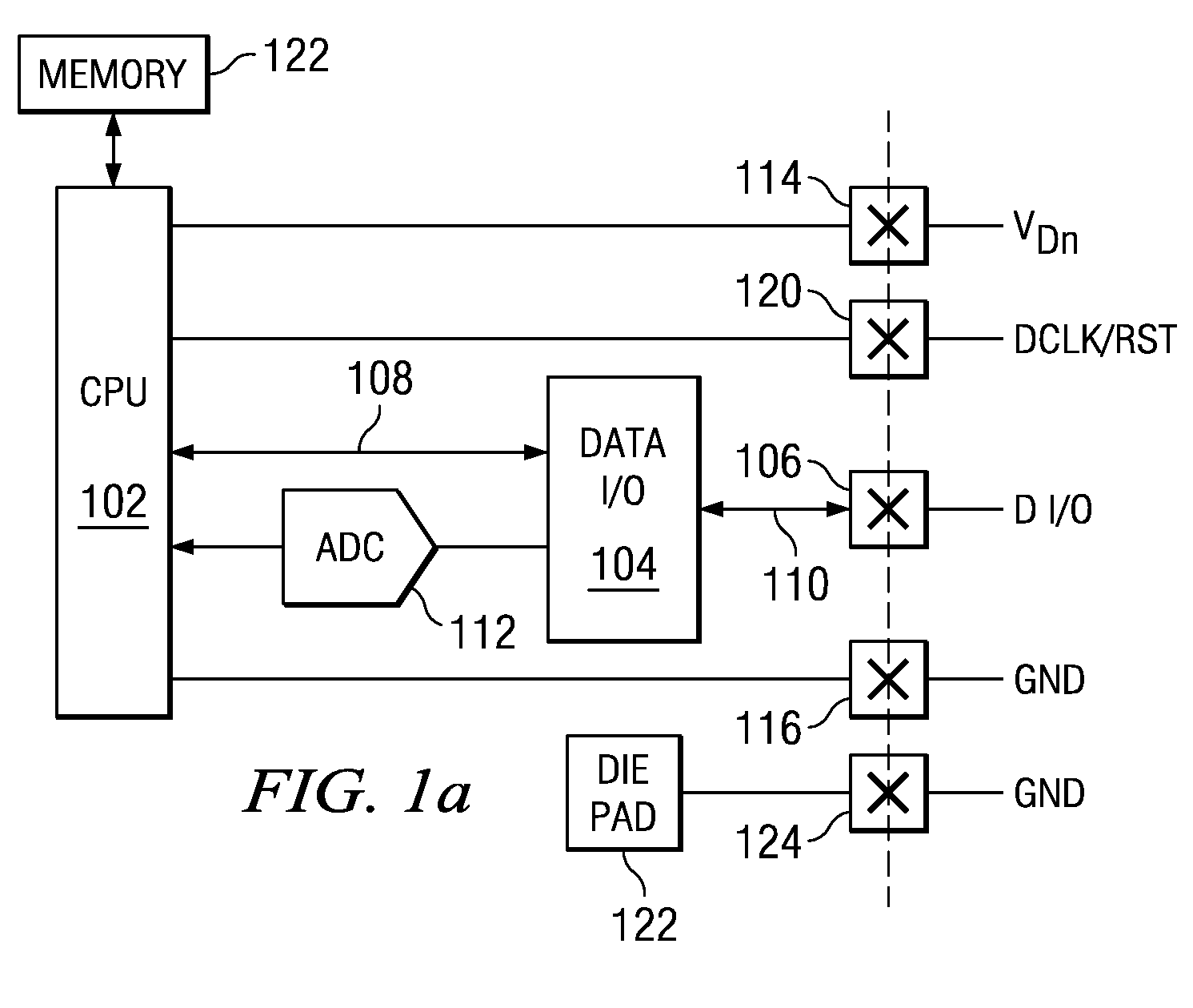
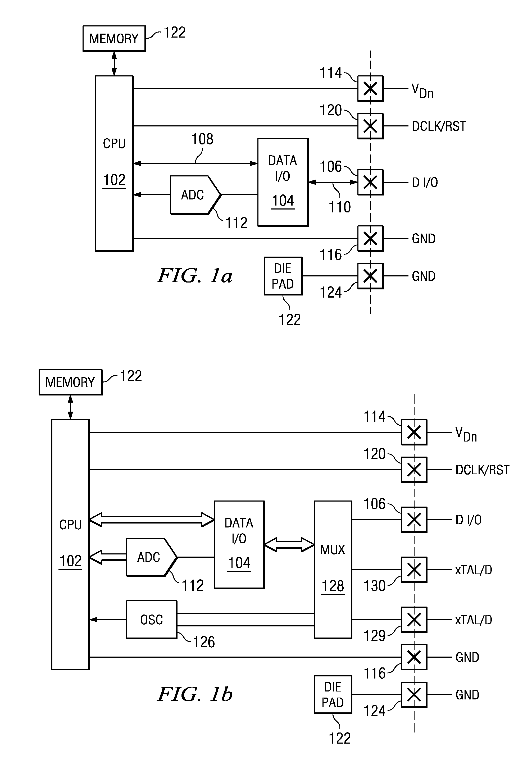
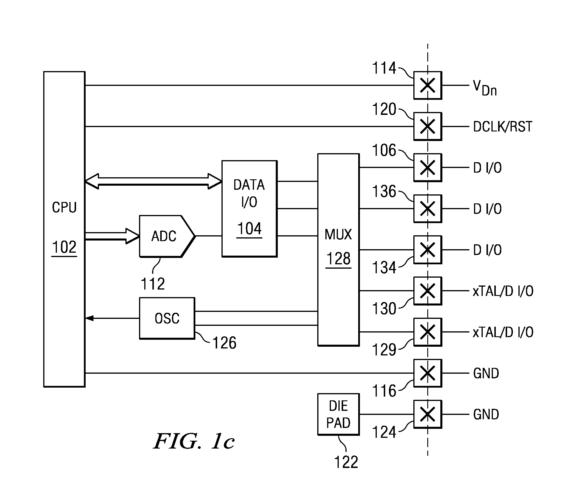
A minimal pin package for a mixed signal integrated circuit for a mixed signal processor based integrated circuit includes a semiconductor chip having a plurality of bond pads disposed thereon with a digital processor digitally interfaceable with at least one of the bond pads. An analog circuit block is provided and interfaceable with at least one of the bond pads. A die pad is provided on which the chip is mounted and N terminals on the package are interfaced to the exterior of the package, one of which is integral with the die pad. Bond wires interface select ones of the bond pads to a supply designated one of the terminals, a ground one of the terminals and the die pad associated with one of the terminals, the rest of the N-3 terminals interfaced to remaining functionality of the chip.

Description

TECHNICAL FIELD OF THE INVENTION[0001]The present invention pertains in general to package devices and, more particularly, to packaging associated with a microcontroller unit (MCU).CROSS-REFERENCE TO RELATED APPLICATIONS[0002]NoneBACKGROUND OF THE INVENTION[0003]As circuit boards become denser and the functionality of the chips increases, the trend toward manufacturing is to dispose a multi function chip with the potential of connecting to multiple output pins in a minimal pin package. Thus, even though multiple outputs could be connected to various input / output pins, it is possible to provide a functional package device that only utilizes certain functions of the chip. Of course, there is a minimal pin count beyond which the chip cannot function. There, of course, must be a power supply input and a ground input, in addition to some kind of data input / output. These data inputs / outputs will be a function of the application in which the chip will be disposed. Additionally, there are s...

Claims


Application Information

Patent Timeline
Patent Type & Authority Applications(United States)
IPC IPC(8): H01L23/48
CPCG06F1/22H01L23/49541H01L23/49548H01L23/5382H01L2224/48091H01L24/48H01L2224/48257H01L2224/49171H01L2924/3011H01L2924/30107H01L24/49H01L2224/48247H01L2924/00014H01L2924/00H01L2224/05554H01L2924/14H01L2924/181H01L2924/00012H01L2224/45099H01L2224/45015H01L2924/207
Inventor LEUNG, KA Y.CZARNOWSKI, JOHN M.HOLBERG, DOUGLAS R.WEST, MATTHEWBANNATYNE, ROSS TODD
Owner SILICON LAB INC
Learn More