Delay selecting circuit for semiconductor memory device

a technology of delay selection and memory device, which is applied in the direction of information storage, static storage, digital storage, etc., can solve the problems of increasing the delay amount applied to the command type of signal for securing the appropriate time margin, and the arrival of the command type of signal very la

Active Publication Date: 2008-04-03
SK HYNIX INC
View PDF7 Cites 47 Cited by
  • Summary
  • Abstract
  • Description
  • Claims
  • Application Information

AI Technical Summary

Benefits of technology

[0015]Embodiments of the present invention are directed to provide a delay selection circuit for preventing a tAA from increasing at a read operation due to a delayed command type of signal.

Problems solved by technology

On the contrary, the command type of signal arrives very late.
That is, with the position of CMD worst, the delay amount applied to the command type of signal for securing the appropriate time margin is increased under the slowest PVT conditions.

Method used


Image

  • Delay selecting circuit for semiconductor memory device
  • Delay selecting circuit for semiconductor memory device
  • Delay selecting circuit for semiconductor memory device

Examples


Embodiment Construction

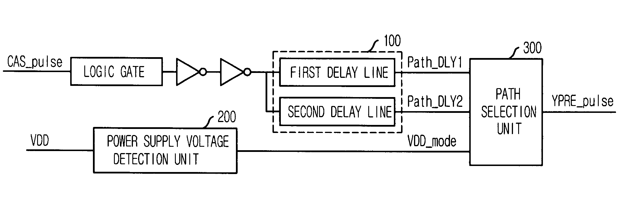
[0027]Under high level of a power supply voltage, a command type of signal is delayed at a writing operation in order to secure a timing margin. However, a tAA is decreased at a reading operation due to a delayed command type of signal. In accordance with the present invention, it is possible to select a delay amount according to a voltage level of the power supply voltage. Therefore, the above-mentioned problem can be prevented. Further, by adding a storing unit, the problem of a command type of signal having two pulses when the power supply voltage is changed during a short time interval can be solved.

[0028]Hereinafter, a delay selection circuit in accordance with the present invention will be described in detail referring to the accompanying drawings.

[0029]FIG. 3 illustrates a block diagram showing a delay selection circuit for use in a semiconductor memory device in accordance with the present invention. The delay selection circuit includes a delay line unit 100, a power supply ...


PUM


Abstract

A delay selection circuit for use in a semiconductor memory device prevents a tAA from increasing at a read operation due to a delayed command type of signal. The delay selection circuit includes a delay line unit, a power supply voltage detection unit and a path selection unit. The delay line unit has two delay lines for delaying a command type of signal by different delay amounts. The power supply voltage detection unit detects a voltage level of a power supply voltage. The path selection unit selects one of each output of the two delay lines according to an output of the power supply voltage detection unit.

Description

CROSS-REFERENCE(S) TO RELATED APPLICATIONS[0001]The present invention claims priority of Korean patent application no. 10-2006-0096303, filed in the Korean Patent Office on Sep. 29, 2006, which is incorporated by reference in its entirety.BACKGROUND OF THE INVENTION[0002]The present invention relates to a semiconductor memory device; and, more particularly, to a semiconductor memory device for preventing discordance of a signal timing, which occurs as a chip size and the number of banks are increased in the semiconductor memory device, between data type of signals and command type of signals.[0003]FIG. 1 illustrates a block diagram showing a semiconductor memory device having eight banks. As capacity of a semiconductor memory device is increased and a semiconductor memory device having high-performance, e.g., a double data rate 3 (DDR3) ram, is developed, a bank structure of the semiconductor memory device has been changed from a conventional 4-bank structure to an 8-bank structure ...

Claims


Application Information

Patent Timeline
Patent Type & Authority Applications(United States)
IPC IPC(8): G11C7/00G11C5/14
CPCG11C5/143G11C7/22G11C7/109G11C7/1078G11C7/1051
Inventor KIM, KYUNG-WHAN
Owner SK HYNIX INC
Why Eureka
Try Eureka