
Systems and methods for electromagnetic band gap structure synthesis

a technology of electromagnetic band gap and structure, applied in the field of electromagnetic band gap structure, can solve the problems of affecting limiting noise, and affecting the design and implementation of these devices, and achieve the effects of improving the performance of ad

Inactive Publication Date: 2008-04-17
GEORGIA TECH RES CORP
View PDF15 Cites 23 Cited by
  • Summary
  • Abstract
  • Description
  • Claims
  • Application Information

AI Technical Summary

Benefits of technology

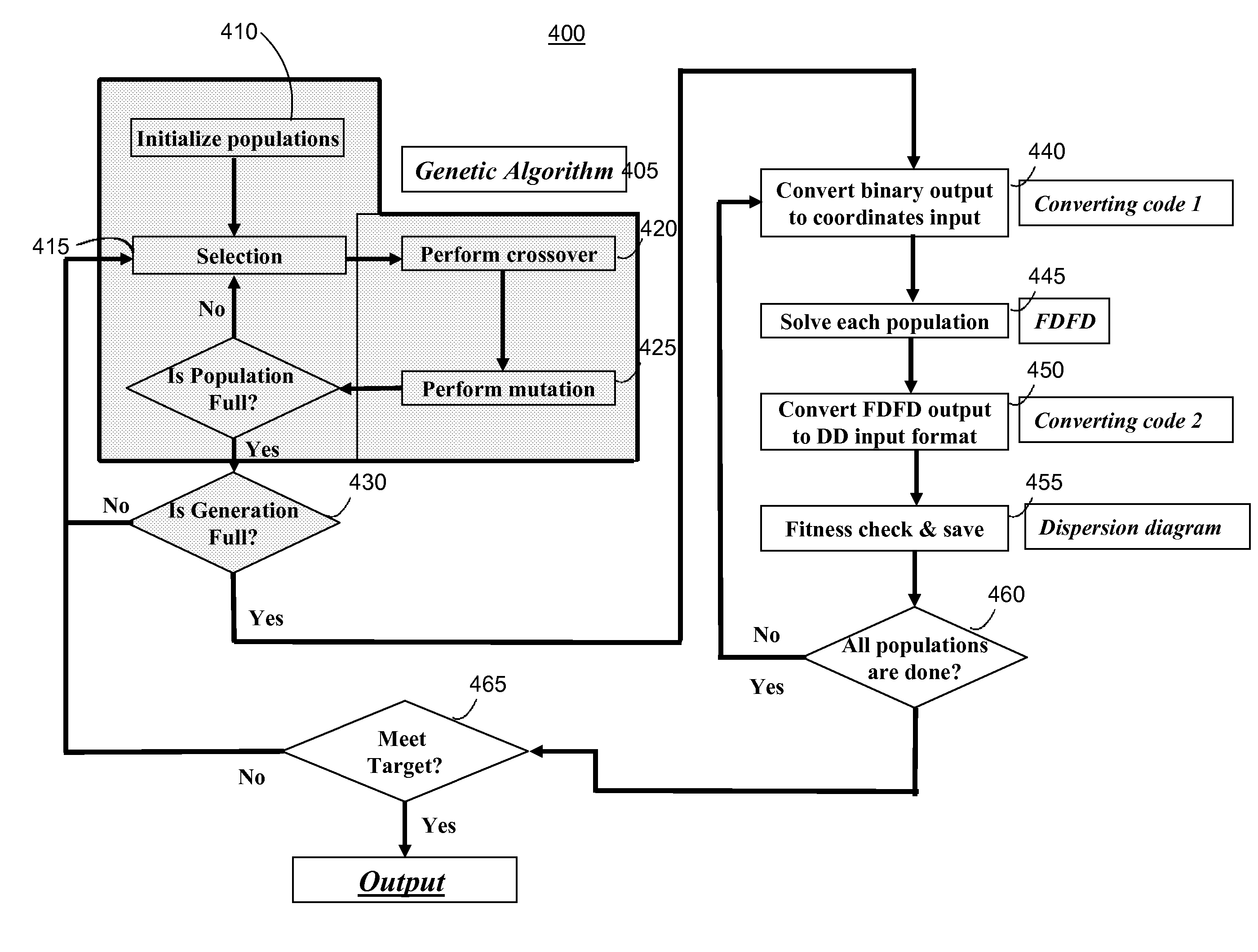
[0017] The present invention describes methods and apparatus for electromagnetic band gap structure synthesis. An exemplary embodiment of the present invention provides a method of electromagnetic band gap structure synthesis, which includes the step of providing a set of desired characteristics for an electromagnetic band gap structure. Furthermore, the method includes generating populations of patch shape members with a genetic algorithm routine and solving one or more of patch shape members of the populations with an electrodynamics modeling technique. Thereafter, the method includes the step of converting the output of the electrodynamics modeling technique into a set of response data for one or more of the patch sh...

Problems solved by technology

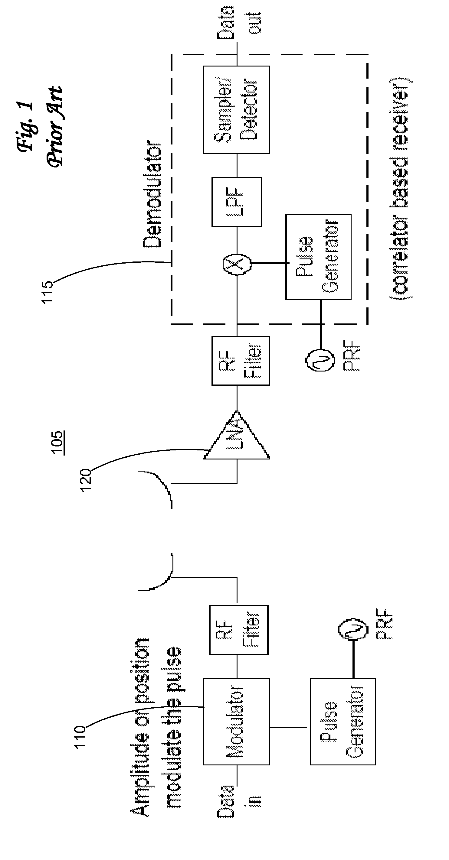
While these high-speed and highly compact devices have created new applications, the design and implementation of these devices have been significantly hindered by increased problems from noise and interference.
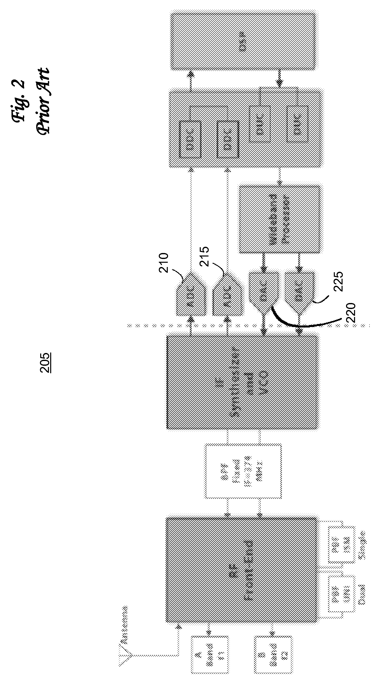
Problems due to noise are especially limiting in devices having both analog circuits and digital circuits, otherwise known as mixed signal systems.
As high-speed and high-resolution ADCs are highly sensitive, a noise spike from digital circuits can affect ADC performance.
This prior art technique is ineffective for many applications, however, because a portion of the electromagnetic energy can still couple through the slot at high frequencies.
Due to the electromagnetic coupling, this method only provides a marginal isolation (i.e., −20 dB to −60 dB) at high frequencies (i.e., above 1 GHz) and becomes ineffective as the sensitivity of the RF circuit increases and the operating frequency of the system increases.
In addition to the failure to be effective at high frequencies, prior art systems with split power / ground planes are ineffective for systems requiring the same DC power supply.
As systems become more complex, multiple power supplies become a luxury a designer cannot afford.
Similar to the prior art technique of splitting the power / ground plane, however, the prior art technique of using ferrite beads for power / ground noise isolation is not effective at high frequencies.
Despite the potential benefits of electromagnetic band gap structures, conventional implementation of these structures is costly and prohibitive.
More particularly, the most popular method of electromagnetic band gap structure design in the prior art involves a manual process that is time consuming, computationally expensive, and unreliable. FIG. 3 provides a block diagram of the conventional manual process of electromagnetic band gap structure synthesis 305.
Furthermore, many input specification sets have no solution.
Therefore, a designer implementing the manual method of electromagnetic band gap structure synthesis 305 may go through hundreds of iterations of the method without ever achieving a satisfactory electromagnetic band gap structure.
The manual method of electromagnetic band gap structure synthesis 305 is computationally expensive and time consuming.
Thus, while electromagnetic band gap structures have the potential to present many advantages in noise suppression applications, there is no method in the prior art that enables reliable and efficient synthesis of these electromagnetic band gap structures.

Method used


Image

  • Systems and methods for electromagnetic band gap structure synthesis
  • Systems and methods for electromagnetic band gap structure synthesis
  • Systems and methods for electromagnetic band gap structure synthesis

Examples


Embodiment Construction

[0045] The present invention addresses the drawbacks of conventional systems and methods of electromagnetic band gap structure synthesis. Significantly, the present invention provides methods and apparatus for efficient and effective electromagnetic band gap structure synthesis. An electromagnetic band gap structure provided in accordance with the present invention is enabled to be accurately and conveniently configured to provide a required isolation level in a predetermined stop band. Additionally, the present invention overcomes the drawbacks of the manual methods in the prior art and provides systems and methods to automatically synthesize electromagnetic band gap structures.

[0046] In an exemplary embodiment, the present invention provides a method of electromagnetic band gap structure synthesis. The method includes the step of providing a set of desired characteristics for an electromagnetic band gap structure. Furthermore, the method includes generating populations of patch s...


PUM


Abstract

The present invention describes methods and apparatus for electromagnetic band gap structure synthesis. An exemplary embodiment of the present invention provides a method of electromagnetic band gap structure synthesis, which includes the step of providing a set of desired characteristics for an electromagnetic band gap structure. Furthermore, the method includes generating populations of patch shape members with a genetic algorithm routine and solving one or more of patch shape members of the populations with an electrodynamics modeling technique. Thereafter, the method includes the step of converting the output of the electrodynamics modeling technique into a set of response data for one or more of the patch shape members and calculating a fitness level for one or more of the sets of response data in comparison to the set of desired characteristics for the electromagnetic band gap structure. Next, the method includes the step of determining whether the fitness level of one of the patch shape members is within a predetermined tolerance. Subsequently, if none of the patch shape members provides a fitness level within the predetermined tolerance, then the steps of generating, solving, converting, calculating, and determining are repeated.

Description

CROSS REFERENCE TO RELATED APPLICATION [0001] This application claims the benefit of U.S. Provisional Application No. 60 / 844,250, filed 13 Sep. 2006, which is hereby incorporated by reference in its entirety as if fully set forth below.FIELD OF THE INVENTION [0002] This invention relates generally to the field of electromagnetic band gap structures, and specifically to systems and methods to efficiently and effectively synthesize electromagnetic band gap structures. BACKGROUND OF THE INVENTION [0003] Explosive developments in microelectronic processing speeds, chip densities, and transmission bandwidths have enabled many new advanced electronic devices. While these high-speed and highly compact devices have created new applications, the design and implementation of these devices have been significantly hindered by increased problems from noise and interference. Problems due to noise are especially limiting in devices having both analog circuits and digital circuits, otherwise known ...

Claims


Application Information

Patent Timeline
IPC IPC(8): G06F17/10
CPCG06F17/5068G06F30/39
Inventor KIM, TAE HONGENGIN, EGESWAMINATHAN, MADHAVAN
Owner GEORGIA TECH RES CORP
Learn More