Interposer, electrical package, and contact structure and fabricating method thereof

Inactive Publication Date: 2008-04-24
IND TECH RES INST
View PDF10 Cites 56 Cited by
  • Summary
  • Abstract
  • Description
  • Claims
  • Application Information

AI Technical Summary

Benefits of technology

[0010]Accordingly, the present invention is directed to a contact structure on a substrate and a

Problems solved by technology

However, along with the drastic increase in the integration of chip's internal circuit, the heat produced by an electrical package carrying the chip has increased accordingly, thus, the problem of improper operation of package device due to thermal stress is always incurred, and mea

Method used


Image

  • Interposer, electrical package, and contact structure and fabricating method thereof
  • Interposer, electrical package, and contact structure and fabricating method thereof
  • Interposer, electrical package, and contact structure and fabricating method thereof

Examples


first embodiment

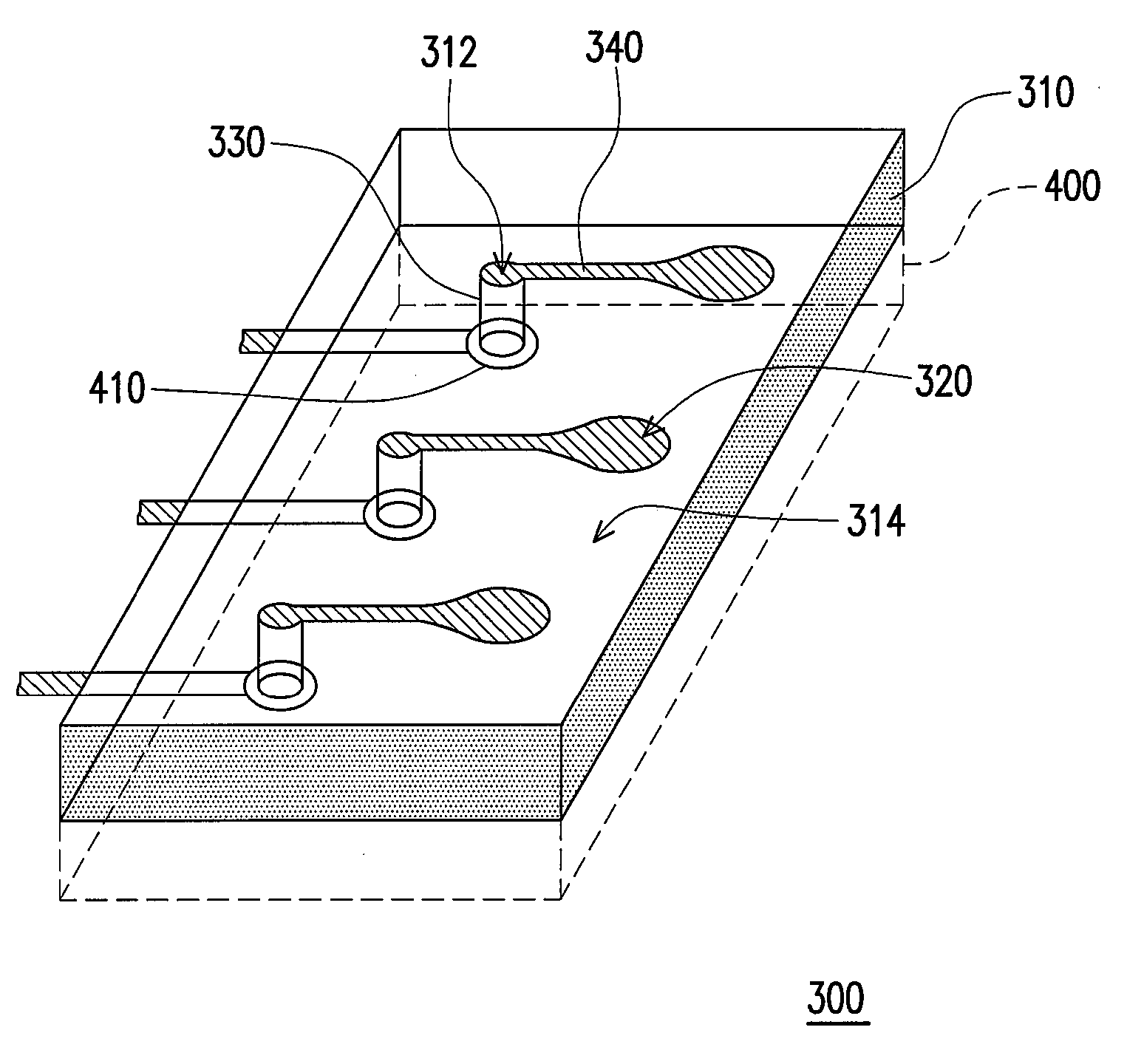
[0035]FIG. 3 is a perspective view of a contact structure on a substrate according to the first embodiment of the present invention. Referring to FIG. 3, the contact structure 300 may be disposed on the substrate 400, and the substrate 400 has at least one contact 410. The contact structure 300 includes a compliant layer 310, at least one solder pad 320, at least one conductive via 330, and at least one conductive arm 340. The compliant layer 310 is disposed on the substrate 400 and covers the contact 410. The conductive via 330 is disposed in the compliant layer 310 and is connected to the contact 410, namely, the conductive via 330 is formed in the through hole 312 which connects two surfaces of the compliant layer 310 and is used for connecting the contact 410 and the conductive arm 340. The solder pad 320 is disposed on the surface 314 of the compliant layer 310 which is in opposite to the substrate 400, and the conductive arm 340 is also disposed on the surface 314 for connecti...

second embodiment

[0042]FIG. 6 is a cross-sectional view of a contact structure according to the second embodiment of the present invention. FIG. 7 is a flowchart illustrating a fabricating method of the contact structure in FIG. 6. FIGS. 8A˜8B are cross-sectional views illustrating the fabrication flow of the contact structure in FIG. 6. In the present embodiment and the first embodiment, similar reference numerals or step numbers refer to similar elements or steps. Only the differences between the two embodiments will be described below.

[0043]Referring to FIG. 6, compared to the first embodiment, the contact structure 300′ in the present embodiment further includes a dielectric layer 350′ disposed on the substrate 400 and exposing a part of the surface of the substrate 400 including the contact 410. The compliant layer 310 covers the part of the surface of the substrate 400. The dielectric layer 350′ may be used for dividing the substrate 400 into a plurality of regions, and the compliant layer 310...

third embodiment

[0046]FIG. 9 is a cross-sectional view of an electrical package according to the third embodiment of the present invention. Referring to FIG. 9, the electrical package 600 includes an interposer 700, a first component 610, and a second component 620. The first component 610 has at least one first contact 612, and the second component 620 has at least one second contact 622.

[0047]As described above, the interposer 700 includes a compliant layer 710, at least one solder pad 720, at least one conductive via 730, and at least one conductive arm 740. The conductive via 730 is disposed in the compliant layer 710 for connecting the second contact 622 and the conductive arm 740. The solder pad 720 is disposed on a surface 712 of the compliant layer 710. The conductive arm 740 is also disposed on the surface 712, and two ends of the conductive arm 740 are respectively connected to the conductive via 730 and the solder pad 720.

[0048]The interposer 700 is disposed between the first component 6...


PUM

PropertyMeasurementUnit
Timeaaaaaaaaaa
Pressureaaaaaaaaaa
Pressureaaaaaaaaaa

Abstract

A contact structure on a substrate which has at least one contact is provided. The contact structure includes a compliant layer, at least one solder pad, at least one conductive via, and at least one conductive arm. The compliant layer is disposed on the substrate and covers the contact. The solder pad is disposed on the surface of the compliant layer which is at the opposite side of the substrate. The conductive via is disposed in the compliant layer and is connected to the contact. The conductive arm is disposed on the surface of the compliant layer in opposite to the substrate, and two ends of the conductive arm are respectively connected to the conductive via and the solder pad. Furthermore, a method for fabricating the contact structure, an interposer and an electrical package using the contact structure are provided.

Description

CROSS-REFERENCE TO RELATED APPLICATION[0001]This application claims the priority benefit of Taiwan application serial no. 95138691, filed Oct. 20, 2006. All disclosure of the Taiwan application is incorporated herein by reference.BACKGROUND OF THE INVENTION[0002]1. Field of the Invention[0003]The present invention relates to the components of an electrical package and a fabricating method thereof. More particularly, the present invention relates to an electrical package of high reliability, an interposer thereof, a contact structure on a substrate, and a fabricating method of the contact structure.[0004]2. Description of Related Art[0005]The operation speed of chips has been improved continuously along with the development in the fabrication technique of integrated circuits (IC), thus, the process and calculation of various digital data has become very efficient. However, along with the drastic increase in the integration of chip's internal circuit, the heat produced by an electrica...

Claims


Application Information

Patent Timeline
IPC IPC(8): H05K1/11H05K3/10
CPCH01L23/49811H05K1/114H05K3/326H05K2201/0133Y10T29/49155H05K2201/09436H05K2201/10378H01L2224/16Y10T29/49165H05K2201/0187H01L2224/05573H01L2224/05568H01L2924/00014H01L2224/0554H01L2224/05599H01L2224/0555H01L2224/0556
Inventor LEE, YUAN-CHANG
Owner IND TECH RES INST
Why Eureka
Try Eureka