Wafer surface bonding technology and semiconductor device structure

A bonding process and device structure technology, applied in semiconductor devices, semiconductor/solid-state device manufacturing, semiconductor/solid-state device components, etc., can solve problems such as poor performance, low degree of dangling bonding, and lack of bonding power

Active Publication Date: 2016-02-17
WUHAN XINXIN SEMICON MFG CO LTD
View PDF5 Cites 4 Cited by
  • Summary
  • Abstract
  • Description
  • Claims
  • Application Information

AI Technical Summary

Problems solved by technology

[0002] During the wafer manufacturing process, due to the lack of bonded Si atoms at the Si interface and the existence of unbonded electrons at the interface Si atoms, electrically active dangling bonds are formed at the Si interface (generally, the crystal lattice suddenly terminates at the surface, and the Each atom of the outermost layer will have an unpaired electron, that is, an unsaturated bond is arranged, and this bond is called a dangling bond (Traps for short), and the bonding degree of this dangling bond is relatively low. There are fewer sources of atoms for bond formation and lack of bonding power, resulting in a lower degree of bonding of dangling bonds between Si interfaces, resulting in poor performance of the device such as DarkCurrent (dark current) and BLC (backlight compensation function)

Method used


Image

  • Wafer surface bonding technology and semiconductor device structure
  • Wafer surface bonding technology and semiconductor device structure
  • Wafer surface bonding technology and semiconductor device structure

Examples


Embodiment Construction

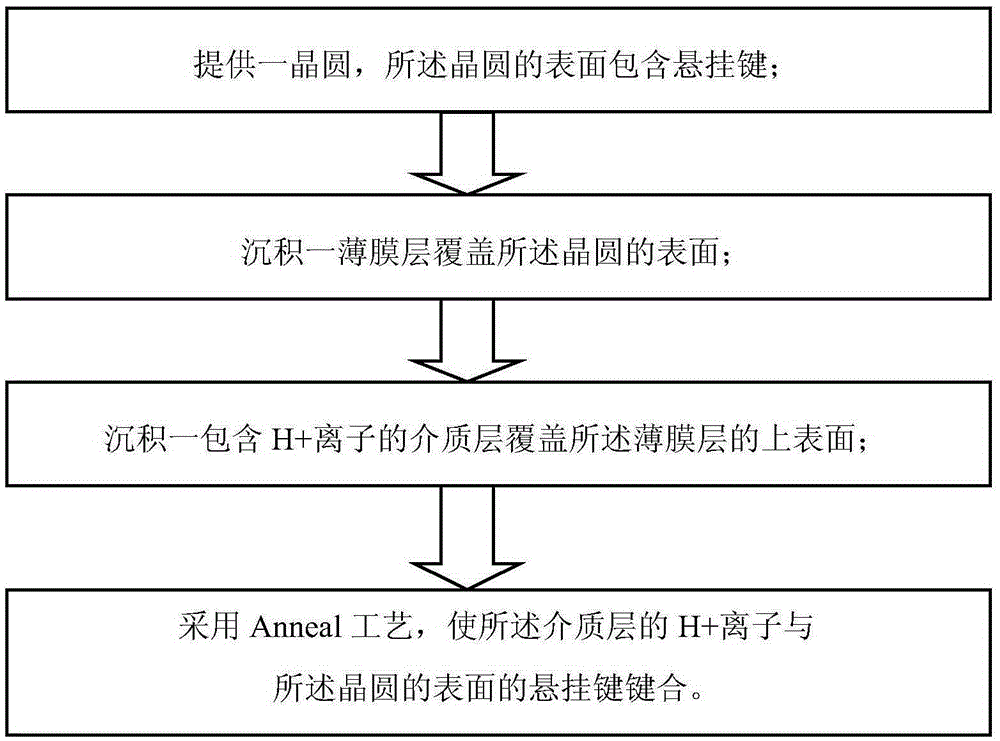
[0026] see figure 1 As shown in the structure, the present invention provides a wafer surface bonding process, which specifically includes:

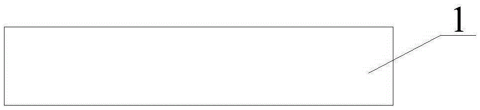
[0027] First, a wafer 1 is provided, the surface of the wafer 1 is made of Si, and the surface of the wafer 1 contains dangling bonds, see Figure 2a shown.

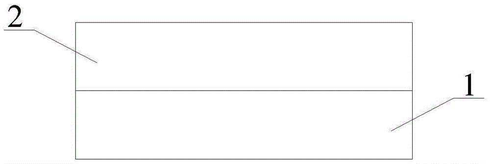
[0028] Secondly, deposit a film layer and cover the surface of wafer 1, preferably, refer to Figure 2b As shown, first deposit a first thin film layer 2, preferably, the first thin film layer 2 is a high-K dielectric layer, wherein the first thin film layer 2 covers the upper surface of the wafer 1; see Figure 2c As shown, a second thin film layer 3 is deposited, preferably, the second thin film layer is a silicon oxide layer, and the second thin film layer 3 covers the upper surface of the first thin film layer 2 .

[0029] Continue to deposit a dielectric layer 4 that contains H+ ions, see Figure 2d As shown, preferably, the dielectric layer 4 is a SiN layer, the dielectri...


PUM


Abstract

The invention relates to the technical field of semiconductor device preparation, and particularly relates to a wafer surface bonding technology and a semiconductor device structure. A thin film layer is deposited on the surface of a wafer, then a dielectric layer including H+ ions is deposited, and finally bonding of the H+ ions in the dielectric layer and wafer Si interface dangling bonds is facilitated through an Anneal technology so that the degree of bonding of the wafer Si interface dangling bonds is enhanced. With application of the technical scheme, Dark Current and BLC performance of the device can be obviously improved.

Description

technical field [0001] The invention relates to the technical field of semiconductor device preparation, in particular to a wafer surface bonding process and a semiconductor device structure. Background technique [0002] During the wafer manufacturing process, due to the lack of bonded Si atoms at the Si interface and the existence of unbonded electrons at the interface Si atoms, electrically active dangling bonds are formed at the Si interface (generally, the crystal lattice suddenly terminates at the surface, and the Each atom of the outermost layer will have an unpaired electron, that is, an unsaturated bond is arranged, and this bond is called a dangling bond (Traps for short), and the bonding degree of this dangling bond is relatively low. There are fewer sources of atoms for bond formation and lack of bonding power, resulting in a lower degree of bonding of dangling bonds between Si interfaces, resulting in poor performance of the device such as DarkCurrent (dark curr...

Claims


Application Information

Patent Timeline
Patent Type & Authority Applications(China)
IPC IPC(8): H01L21/50H01L23/10
CPCH01L24/29H01L24/83H01L2224/2957H01L2224/83375
Inventor 王喜龙胡胜邹文王言虹
Owner WUHAN XINXIN SEMICON MFG CO LTD
Why Eureka
Try Eureka