Photodiode array and method for making thereof

Active Publication Date: 2008-04-24
HAMAMATSU PHOTONICS KK
View PDF6 Cites 2 Cited by
  • Summary
  • Abstract
  • Description
  • Claims
  • Application Information

AI Technical Summary

Benefits of technology

[0007] The present invention provides a photodiode array capable of being formed by a simple step and

Problems solved by technology

The greatest problem of the multichannel photodiode

Method used


Image

  • Photodiode array and method for making thereof
  • Photodiode array and method for making thereof
  • Photodiode array and method for making thereof

Examples


Example

[0031] Hereafter, a photodiode array according to an embodiment of the present invention will be explained. Identical components are designated by the same reference numerals, and overlapping description is omitted.

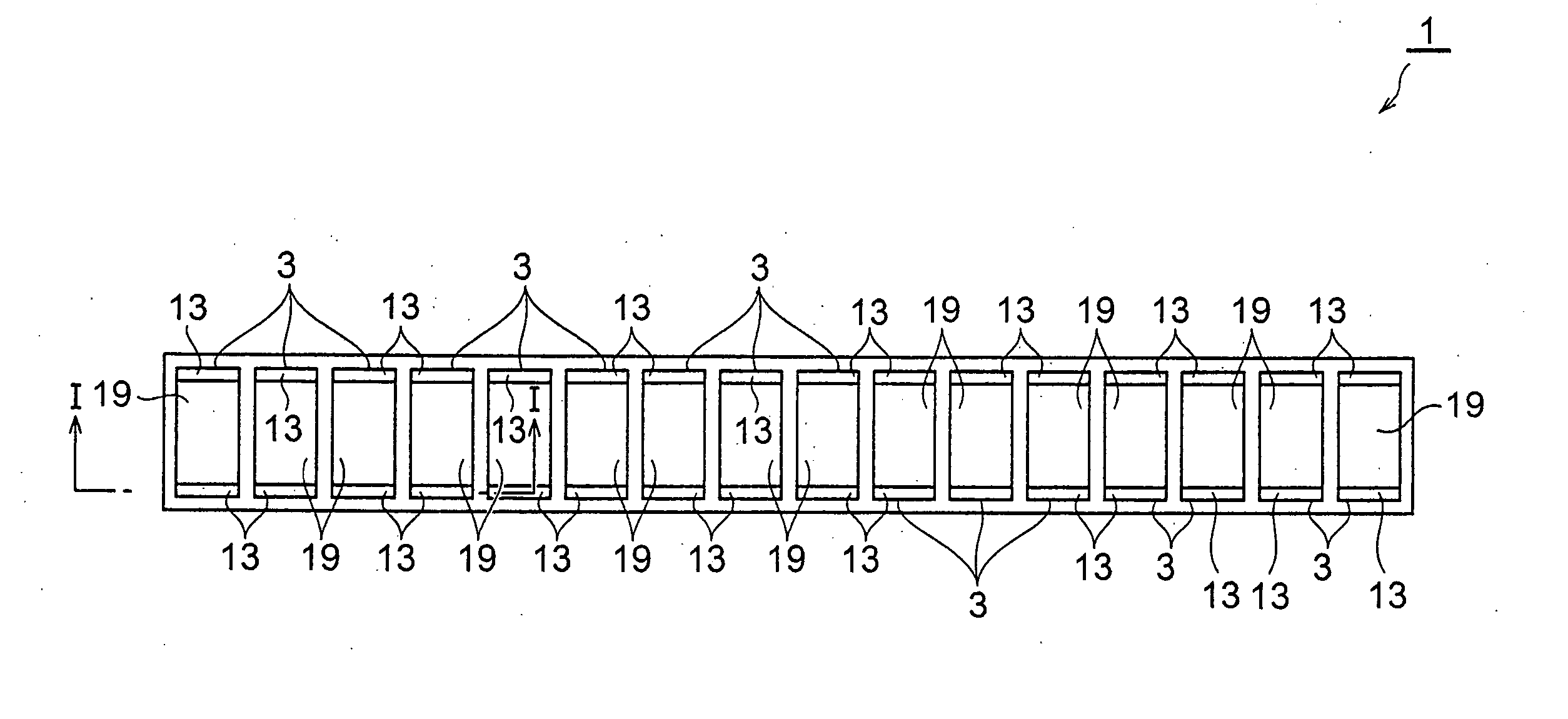
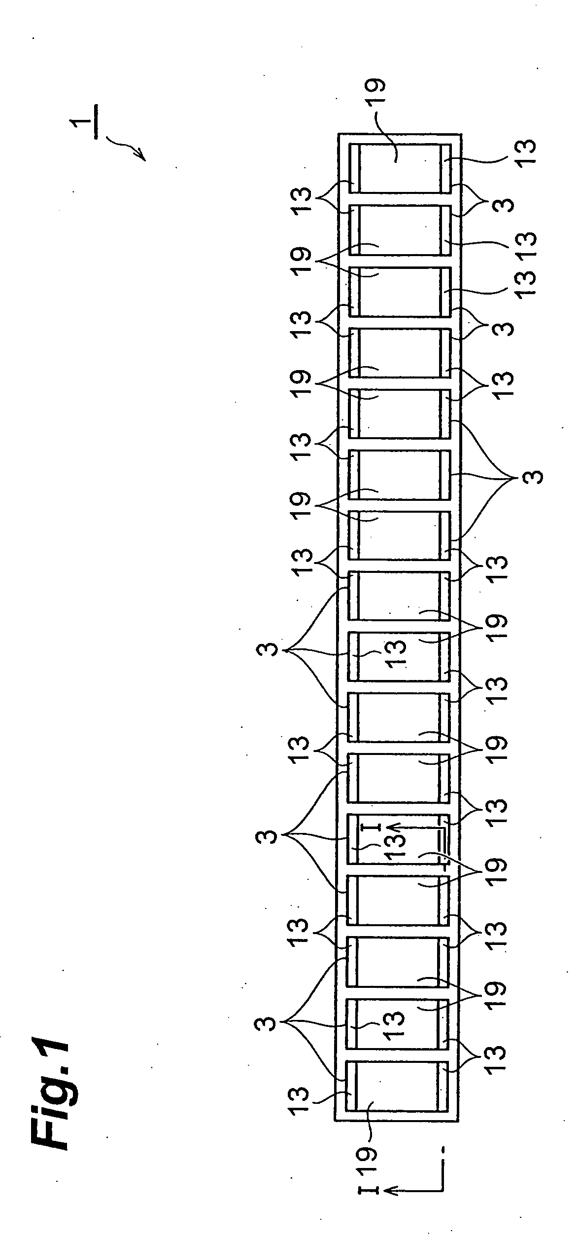
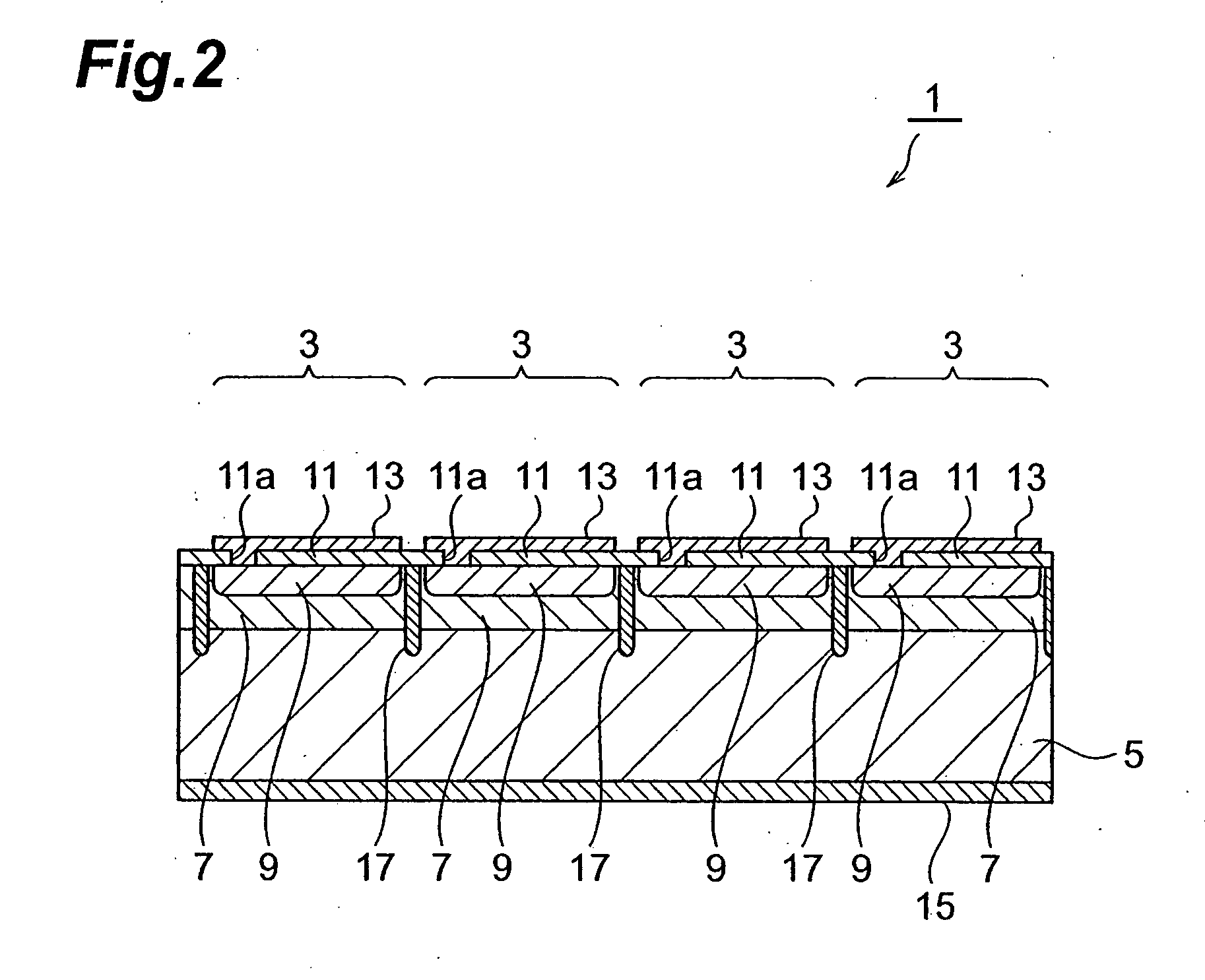
[0032]FIG. 1 is a plan view showing an embodiment of a photodiode array according to the present invention. FIG. 2 is a sectional view showing the I-I section of the photodiode array shown in FIG. 1. In the photodiode array 1 according to the embodiment, a plurality of photodiodes 3, for embodiment, of 16 pieces are one-dimensionally arranged.

[0033] With reference to FIG. 1, each of the photodiodes 3 has a photodetecting region 19. The photodiode 3 has a surface electrode 13 formed at the both ends of the photodetecting region 19.

[0034] With reference to FIG. 2, the photodiode array 1 is provided with a semiconductor substrate 5 consisting of an n-type semiconductor, a first semiconductor layer 7 formed on the semiconductor substrate 5 and consisting of a semiconductor...


PUM


Abstract

Disclosed is a photodiode array comprising a semiconductor substrate; a plurality of photodiodes formed on the semiconductor substrate; and crystal fused regions losing crystallinity by fusing a semiconductor material of the photodiodes between the plurality of photodiodes.

Description

BACKGROUND OF THE INVENTION [0001] 1. Field of the Invention [0002] The present invention relates to a photodiode array. [0003] 2. Related Background of the Invention [0004] A multichannel photodiode and a photodiode array have been known as a photodetecting element having a plurality of pixel regions formed on the same substrate. The greatest problem of the multichannel photodiode and photodiode array is cross talk between pixels. [0005] As a method for preventing cross talk between the pixels, for embodiment, a structure where trench grooves are formed between the pixels and the trench grooves are filled with an insulating material to maintain the mechanical strength is disclosed in Japanese Patent Laid-Open Publication No. 2001-352094. FIG. 13 is a sectional view showing a photodiode array disclosed in Japanese Patent Laid-Open Publication No. 2001-352094. With reference to FIG. 13, a photodiode array 100 is provided with a plurality of photodiodes 101. The photodiode 101 consist...

Claims


Application Information

Patent Timeline
IPC IPC(8): H01L31/02
CPCH01L27/1443H01L27/14683H01L27/1463H01L27/1446
Inventor FUJII, YOSHIMAROOKAMOTO, KOUJISAKAMOTO, AKIRA
Owner HAMAMATSU PHOTONICS KK
Why Eureka
Try Eureka