Semiconductor chip package and fabrication method thereof
Inactive Publication Date: 2007-04-26
LAPIS SEMICON CO LTD
View PDF2 Cites 0 Cited by
Summary
Abstract
Description
Claims
Application Information
AI Technical Summary
This helps you quickly interpret patents by identifying the three key elements:
Problems solved by technology
Method used
Benefits of technology
Benefits of technology
[0027] According to the semiconductor chip package fabrication method of the present invention, acceleration sensor chip packages are fabricated in simple steps, and yield can be remarkably improved.
[0028] The MEMS chips (first semiconductor chips) of the package are individually separated after the first sealing section is formed for each chip on the wafer level. Thus, only if the semiconductor substrate is positioned, positioning for each chip is unnecessary when making the first sealing section. Because the positioning for each chip is unnecessary, positioning accuracy, that is repeatability, can be improved. As a result, the first sealing section can be accurately formed. Therefore an improvement of yield and productivity of MEMS chips and the package including the MEMS chips can be achieved.
Problems solved by technology
Therefore, seal-by-potting using transfer mold or liquid resin cannot be performed, and the area of the package increases.
This will hinder the operation of the movable element.
As Japanese Patent Application Kokai No. 7-225240 discloses, for example, attaching a special member to the acceleration sensor chip makes the fabrication steps more complicated.
This worsens the throughput not only of the acceleration sensor chip, but also of the acceleration sensor chip package, which is the final product.
Method used
Image
Click on the blue label to locate the original text in one second.
Reading with bidirectional positioning of images and text.
Examples
first embodiment
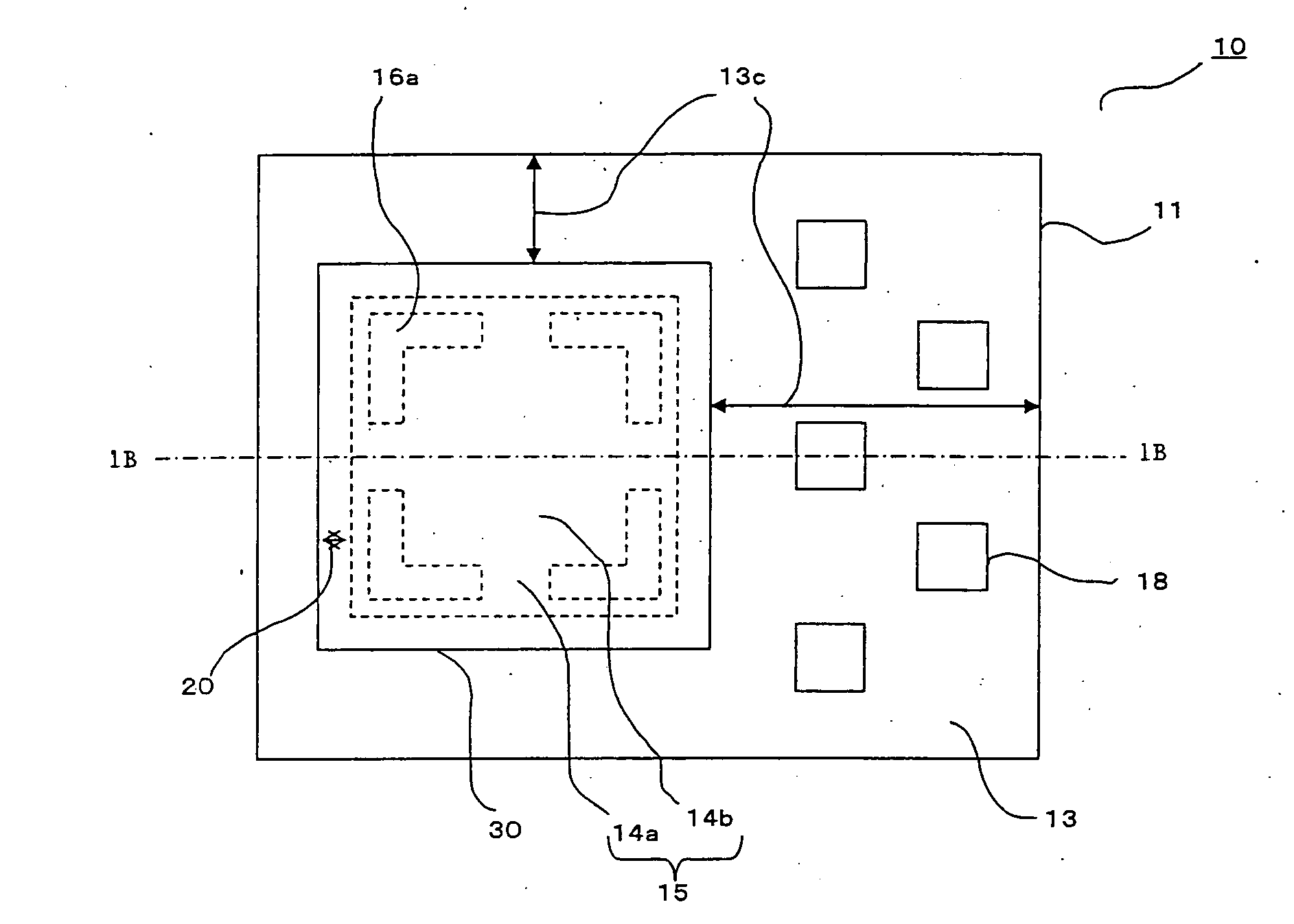
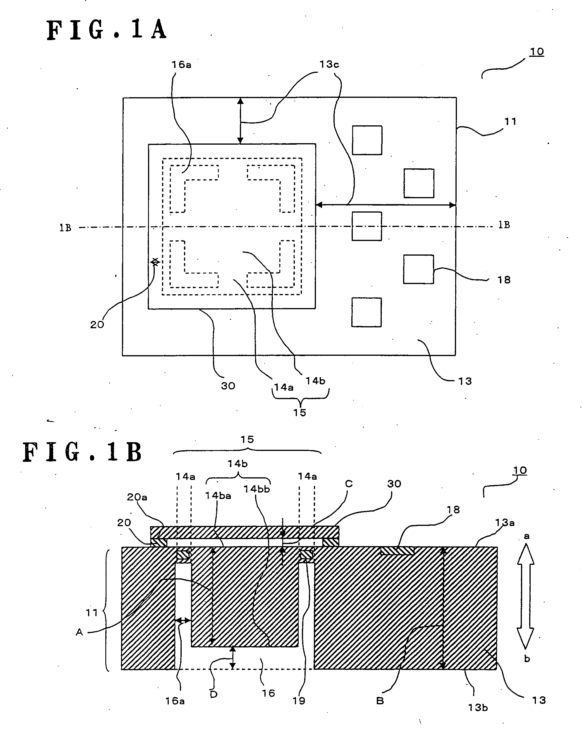
[0063] First a configuration example of the semiconductor chip of the present invention will be described with reference to FIG. 1A and FIG. 1B. Here a piezo acceleration sensor chip having a piezo resistance element as the functional element will be described.
[0064] Here the acceleration sensor chip is a chip that can measure acceleration (hereafter also called “chip”), and the acceleration sensor chip package is a packaged device including this acceleration sensor chip.
[0065]FIG. 1A illustrates the composing elements of the semiconductor chip of this embodiment viewed from the top.
[0066] As FIG. 1A and FIG. 1B show, the first semiconductor chip 10 includes a chip 11. The chip 11 includes a frame section 13 having the top face 13a and the bottom face 13b. The bottom face 13b is generally in parallel to the top face 13a. The frame section 13 is a square frame defining the outer shape (contour) of the chip 11.
[0067] The chip 11 has the opening section 16. In this embodiment, the ...
second embodiment
[0120] The second embodiment of the present invention will be described with reference to FIGS. 6A and 6B. The second embodiment relates to a packaged semiconductor device including the semiconductor chip having the configuration described above.
[0121]FIG. 6A depicts the composing elements of the semiconductor chip package of the second embodiment viewed from the top. FIG. 6B is a cross-section sectioned at the dashed line 6B-6B in FIG. 6A.
[0122] The semiconductor chip package of this embodiment is characterized in that the ceramic header is used for the substrate on which the semiconductor chip is mounted.
[0123] The ceramic header is a ceramic substrate having a concave section in which the semiconductor chip is received and mounted. Thus, the ceramic header is a container type ceramic substrate.
[0124] As FIG. 6A and FIG. 6B show, the semiconductor chip package 1 includes the ceramic header 40.
[0125] The ceramic header 40 has a first main surface 40a and a second main surface ...
third embodiment
[0153] A semiconductor device according to the third embodiment of the present invention will be described with reference to FIG. 7A and FIG. 7B. The third embodiment relates to a packaged semiconductor device having a metal or resin substrate instead of the ceramic header of the second embodiment.
[0154]FIG. 7A depicts the composing elements of the semiconductor chip package of the third embodiment viewed from the top. FIG. 7B is a cross-section sectioned at the dashed line 7B-7B in FIG. 7A. In FIG. 7A, the second sealing section shown in FIG. 7B is omitted to clarify the internal configuration.
[0155] In the following description, the same or similar components in the semiconductor device 1 of the present embodiment as the semiconductor device of the second embodiment are not described in detail. The same or similar composing elements are denoted with the same reference numbers in FIGS. 6A, 6B, 7A and 7B.
[0156] The semiconductor chip package 1 includes the substrate 40. For the b...
PUM
Abstract
A semiconductorchippackage includes a first semiconductorchip, that is an MEMS chip having a movable structure. The movable structure has a movable section. The first semiconductor chip includes a plurality of first electrode pads, and a first sealing section. The first sealing section is a closed loop formed on the top face of the frame section surrounding the movable structure. The first semiconductor chip also includes a thin plate member for sealing the movable structure. The semiconductor chippackage also includes a second semiconductor chip. The second semiconductor chip has a plurality of second electrode pads. The semiconductor chip package also includes a substrate. The substrate has third electrode pads. The first and second semiconductor chips are mounted on the substrate. First bonding wires connect the first electrode pads to the second electrode pads. Second bonding wires connect the second electrode pads to the third electrode pads.
Description
BACKGROUND OF THE INVENTION [0001] 1. Field of the Invention [0002] The present invention relates to a semiconductor chip package and a fabrication method thereof. [0003] 2. Description of the Related Art [0004] Technology to fabricate a several hundred μm size micro structure using micro machining technology, such as semiconductor micro processing technology, has been developing. For example, application of this technology to various sensors, optical switches in the optical communication field and radio frequency (RF) components has begun. [0005] Such micro structures can be fabricated using a conventional semiconductor fabrication process, so that it can be integrated into a single chip. [0006] A chip on which a system having specific functions, including this micro structure, is constructed is called a Micro-Electrical-Mechanical System (MEMS) chip, or a Micro-System-Technology (MIST) chip (hereafter simply called an MEMS device). One example of known MEMS devices is an accelerat...
Claims
Application Information
Patent Timeline
Application Date:The date an application was filed.
Publication Date:The date a patent or application was officially published.
First Publication Date:The earliest publication date of a patent with the same application number.
Issue Date:Publication date of the patent grant document.
PCT Entry Date:The Entry date of PCT National Phase.
Estimated Expiry Date:The statutory expiry date of a patent right according to the Patent Law, and it is the longest term of protection that the patent right can achieve without the termination of the patent right due to other reasons(Term extension factor has been taken into account ).
Invalid Date:Actual expiry date is based on effective date or publication date of legal transaction data of invalid patent.

