Storage device and storing method

Inactive Publication Date: 2008-04-24
HITACHI LTD
View PDF1 Cites 81 Cited by
  • Summary
  • Abstract
  • Description
  • Claims
  • Application Information

AI Technical Summary

Benefits of technology

[0019]The present invention is adapted to cause the flash drive to inform the superior controlling unit on the maximum value of the number of deletion of a deletion unit, and cause the superio

Problems solved by technology

The methods can prolong the lifetime, however, cannot eliminate the lifetime.
As there is a technique for prolonging a lifetime of the flash memory in the conventional art, it is impossible to eliminate the lifetime.
At that moment, a failure occurs that a part of the flash memory is impossible to be deleted or written.
The management of the logical address and the physical address is performed by the superior system, there is a pr

Method used


Image

  • Storage device and storing method
  • Storage device and storing method
  • Storage device and storing method

Examples


embodiment 1

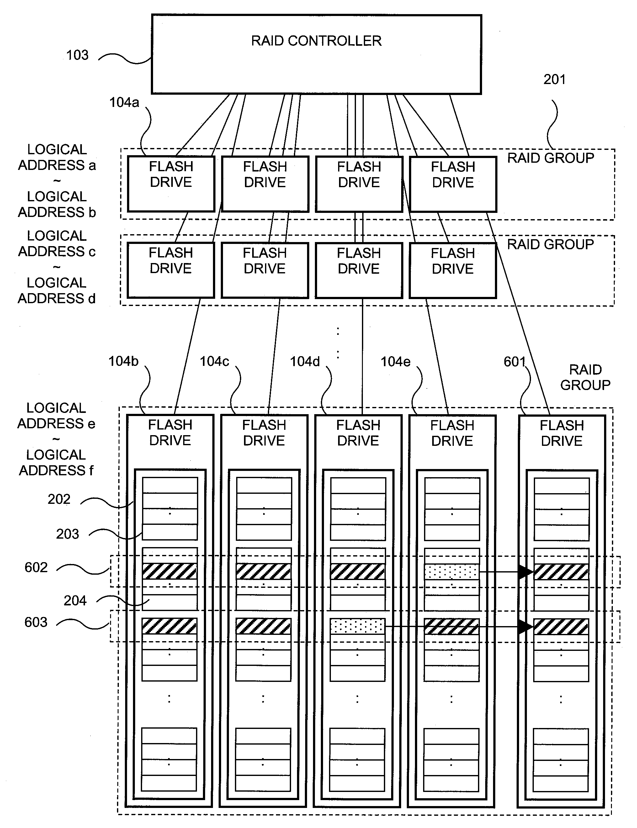
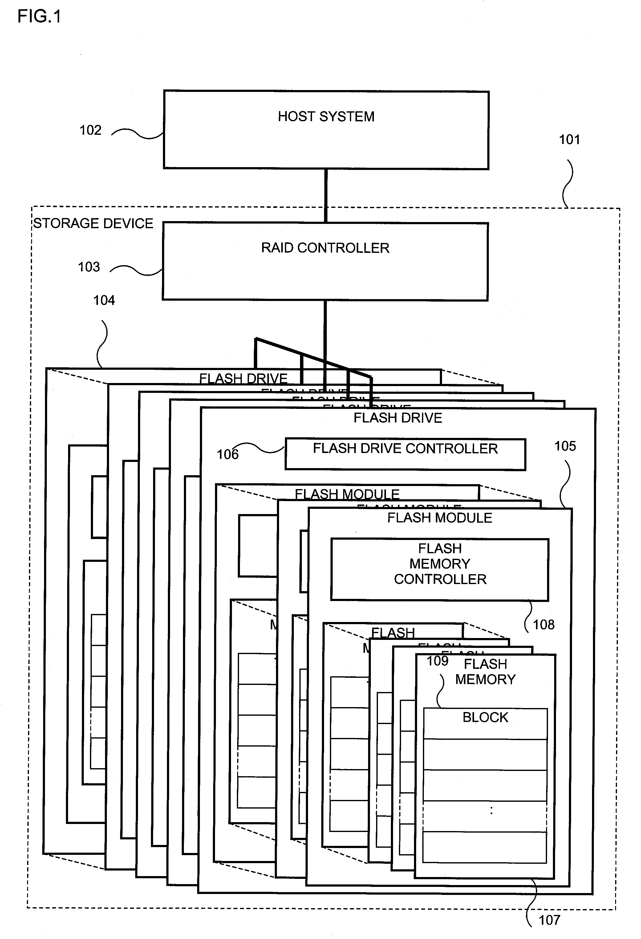
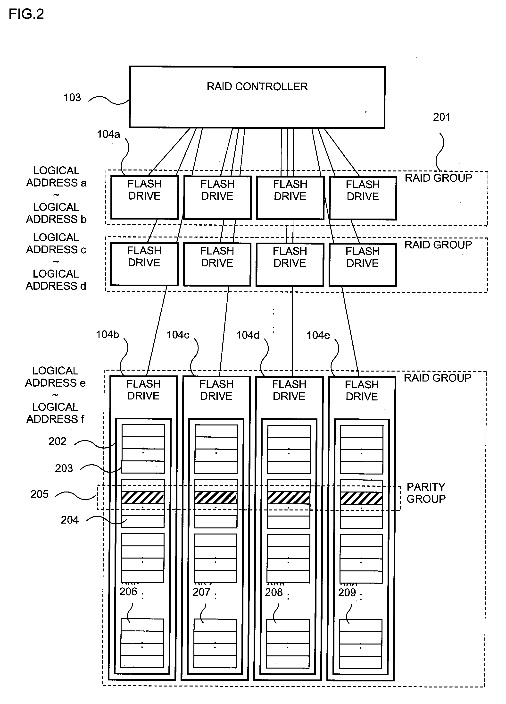
[0038]The first embodiment of the present invention will be described by using FIGS. 1 to 6 and FIGS. 8, 9, and 11. FIG. 1 shows a configuration of a storage device 101 of the embodiment. The storage device 101 includes a plurality of flash drives 104 and a RAID controller 103, which controls the plurality of flash drives 104 in the storage device 101. The storage device 101 is connected to a host system 102 via the RAID controller 103.

[0039]The flash drive 104 includes a plurality of flash modules 105, each of which is a printed board provided with a plurality of flash memory devices 107 and a flash memory controller 108. A flash drive controller 106 interfaces exchanges between the flash module 105 and the RAID controller 104, the superior controlling unit of the flash module 105.

[0040]The storage device 101 that puts much stress on reliability has a plurality of flash drives 104, for example, with four flash drives forming a RAID group 201. The RAID controller 103 allocates a log...

embodiment 2

[0075]The same thing can be done also in a flash module in a flash drive. That is to say, before deletion units that cannot to be deleted increase in a flash memory device to make it unable to address writing, a flash module is added and caused to substitute for the flash memory that is unable to address writing.

[0076]The second embodiment of the present invention will be described by using FIGS. 7, 10, and 12. A flash memory is added by the unit of the flash drive in the first embodiment; while a flash memory is added by the unit of a flash module in the flash drive in the second embodiment.

[0077]The flash module has a structure of a printed board provided with a plurality of flash memory devices and a controller for converting a logical address in the flash memory module and a physical address of the flash memory.

[0078]A flash drive controller for controlling a plurality of flash modules is in the flash drive.

[0079]In the first embodiment, the RAID position information is present ...


PUM


Abstract

To enable a capacity of an entire storage device to be kept by adding a flash drive or a flash module in the flash drive for a flash memory that has a failure, even if the storage device using the flash memory has a failure in its part such as a part of flash memory chip has a failure, for example, the flash memory chip has run out of its lifetime. In a storage device 101 equipped with two or more memory device units 105 with a plurality of semiconductor memory devices 107, each of which has a functional capacity unit 109 smaller than a capacity of an entire semiconductor memory device and has a writing lifetime for each functional capacity unit, only a functional capacity unit whose writing lifetime is run out to be determined as unable to be written is substituted by a functional capacity unit in a memory device of the other memory device unit to keep a predetermined capacity of the entire device.

Description

[0001]The present application is based on and claims priority of Japanese patent application No. 2006-286108 filed on Oct. 20, 2006, the entire contents of which are hereby incorporated by reference.BACKGROUND OF THE INVENTION[0002]1. Field of the Invention[0003]The present invention relates to a storage device and a storing method, and more specifically, to a controlling method and an implementing method of a flash memory for enhancing reliability of a storing system using a flash memory.[0004]2. Description of the Related Art[0005]As a non-volatile semiconductor memory, there is a flash memory for which a deletion unit or a writing unit (functional capacity unit) is previously determined. The flash memory has a floating gate structure, which wraps a conductor such as a polysilicon in an oxide insulator such as an oxide silicon for storing information by the presence of the charge, which is in the floating gate. The flash memory may use a structure for reserving a charge in a parti...

Claims


Application Information

Patent Timeline
IPC IPC(8): G06F12/00G06F12/16
CPCG11C16/3495G11C29/765G11C29/76G06F3/0688G06F3/0616G06F3/064
Inventor KITAHARA, JUN
Owner HITACHI LTD
Why Eureka
Try Eureka