LED backlight with bare chip LED

a technology of led backlight and chip, which is applied in the field of backlight light sources, can solve the problems of limited life time, relatively high power consumption, and low efficiency of light emitting diodes (leds), and achieve the effect of reducing separation

Inactive Publication Date: 2008-05-01
K LASER TECH
View PDF8 Cites 42 Cited by
  • Summary
  • Abstract
  • Description
  • Claims
  • Application Information

AI Technical Summary

Benefits of technology

[0009]The present invention provides a method and apparatus which uses the edge emitting characteristics of the LED bare chip to form a backlight with uniform illumination. This allo...

Problems solved by technology

Although a CCFL is a good light source for a LCD, its power consumption is relatively high and its life time is limited (to ap...

Method used


Image

  • LED backlight with bare chip LED
  • LED backlight with bare chip LED
  • LED backlight with bare chip LED

Examples


Embodiment Construction

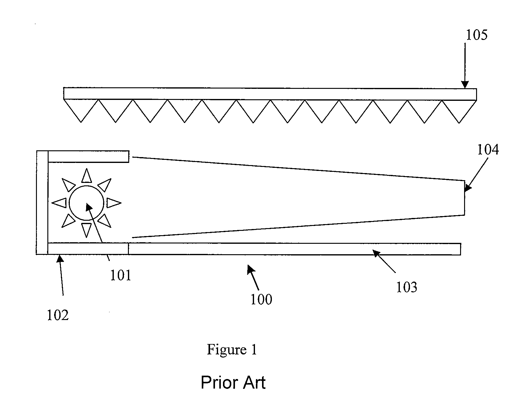
[0025]FIG. 6 shows a side view of a prior art LED bare chip 600. A junction layer 60225 is grown on top of a substrate 601. When an electric current passes through the junction layer, light will be emitted from the junction as shown in FIG. 6(a). FIG. 6(b) shows the top view of LED chip 600. It can be seen that light is emitting from the four sides of the chip. This is the most common technique in fabricating a LED. An LED can be fabricated to emit light from the top surface also. However, the process is more complicated and thus has a higher manufacturing cost. Yet the surface emitting type LED has no advantage in the scheme of this present invention. In a commercially available LED package, the bare chip is often molded inside a high index plastic which serves as light guide to cause the LED to project light upwards.

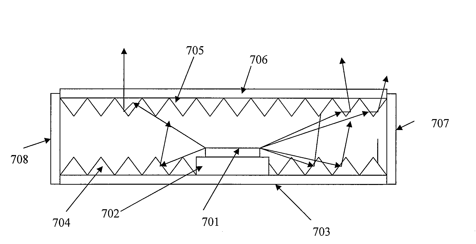
[0026]FIG. 7 shows a backlight unit with a single LED bare chip according to an embodiment of the invention. It illustrates how to convert the light emitting from the ...


PUM


Abstract

A method and apparatus which uses the edge emitting characteristics of the LED bare chip to form a backlight with uniform illumination. This allows a reduced separation between the diffuser plate and the LED array. In one embodiment, the LED chip(s) is mounted over a prism structure, which redirects the side emitted light outwards.

Description

CROSS-REFERENCES TO RELATED APPLICATIONS[0001]NOT APPLICABLEBACKGROUND OF THE INVENTION[0002]The present invention relates to backlight light sources for a Liquid Crystal Display (LCD), and in particular a Light Emitting Diode (LED) light source.[0003]Most modern color LCDs must be viewed with a light source behind the LCD panel. This light source is usually called a Backlight. At present, most applications use a Cold Cathode Fluorescent Lamp (CCFL) as light source for the backlight. This lamp emits light inside a tubular structure.[0004]FIG. 1 shows a side, cut-away view of a typical backlight unit 100 using a CCFL 101 which is housed in a reflective box 102. There is an opening on one side for the lamp to project light into a light guide 104. A prism film 105 is used to redirect the light towards the surface of the LCD. A reflective surface 103 is used behind the light guide to reflect stray light toward the LCD.[0005]As shown in FIG. 2, in order to provide a more intense illumina...

Claims


Application Information

Patent Timeline
IPC IPC(8): F21V7/04F21K99/00H01L33/48H01L33/60H01L33/62
CPCG02B5/045G02F2001/133607G02F1/133605G02F1/133603G02F1/133607
Inventor LEE, WAI-HON
Owner K LASER TECH
Why Eureka
Try Eureka