Compensating for layout dimension effects in semiconductor device modeling

a semiconductor device and layout dimension technology, applied in the field of semiconductor device manufacturing, can solve the problems of inability to manufacture devices, degree of inaccuracy, and increasing the effect of the performance of the completed devices

Inactive Publication Date: 2008-05-01
ADVANCED MICRO DEVICES INC
View PDF6 Cites 12 Cited by
  • Summary
  • Abstract
  • Description
  • Claims
  • Application Information

AI Technical Summary

Benefits of technology

[0012]The following presents a simplified summary of the invention in order to provide a basic understanding of some aspects of the invention. This summary is not an exhaustive overview of the invention. It is not intended to identify key or critical elements of the invention or to delineate the scope of the invention. Its sole purpose is to present some concepts in a simplified form as a prelude to the more detailed description that is discussed later.

Problems solved by technology

However, in actual fabricated devices, the devices are not fabricated as shown in the ideal geometries of FIGS. 1A and 1B.
Modeling the devices 100, 120 using ideal length and width parameters results in some degree of inaccuracy, because it does not account for the corner rounding.
As device geometries continually decrease, these small modeling inaccuracies have an increasingly noticeable effect on the performance of the completed devices.

Method used


Image

  • Compensating for layout dimension effects in semiconductor device modeling
  • Compensating for layout dimension effects in semiconductor device modeling
  • Compensating for layout dimension effects in semiconductor device modeling

Examples


Embodiment Construction

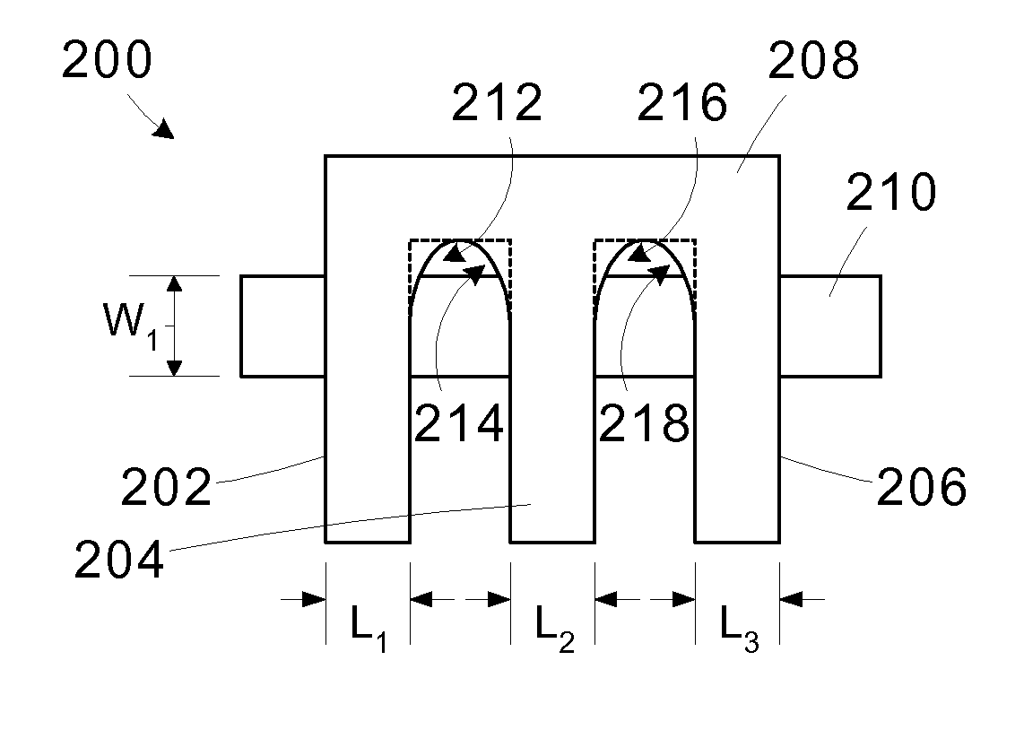
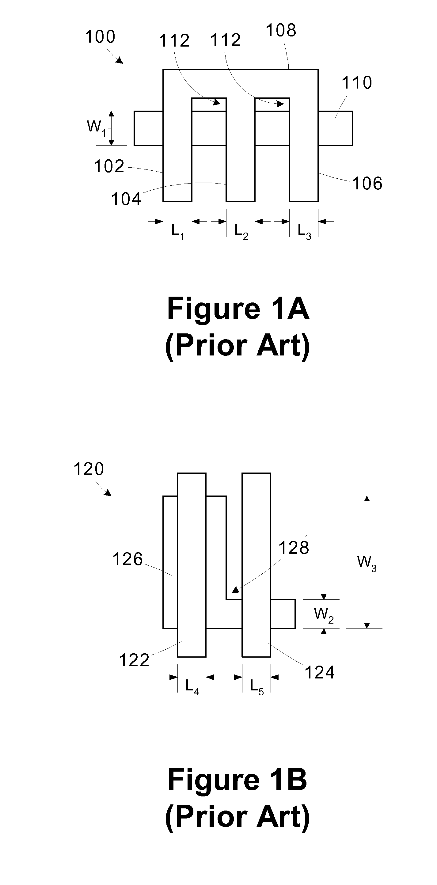
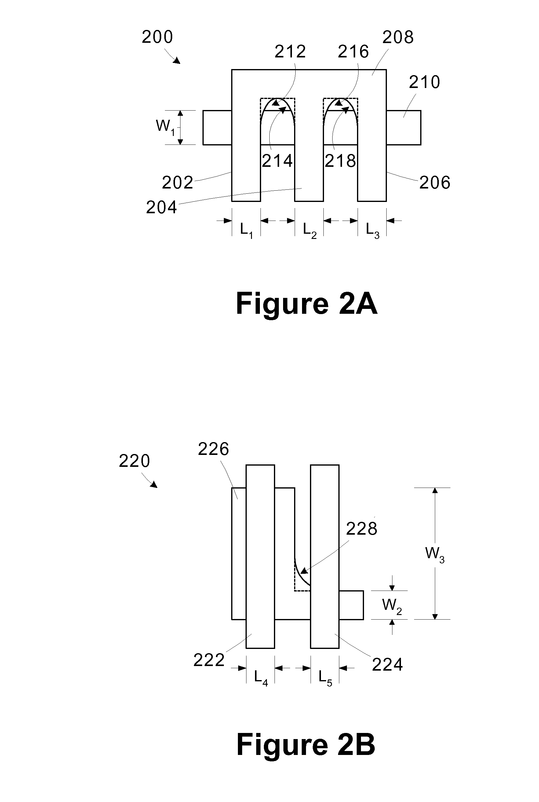
[0022]One or more specific embodiments of the present invention will be described below. It is specifically intended that the present invention not be limited to the embodiments and illustrations contained herein, but include modified forms of those embodiments including portions of the embodiments and combinations of elements of different embodiments as come within the scope of the following claims. It should be appreciated that in the development of any such actual implementation, as in any engineering or design project, numerous implementation-specific decisions must be made to achieve the developers' specific goals, such as compliance with system-related and business related constraints, which may vary from one implementation to another. Moreover, it should be appreciated that such a development effort might be complex and time consuming, but would nevertheless be a routine undertaking of design, fabrication, and manufacture for those of ordinary skill having the benefit of this...


PUM


Abstract

A method includes receiving design data associated with an integrated circuit device. The integrated circuit device includes a first element having a corner defined therein and a second element overlapping the first element. A dimension specified for the first element in the design data is adjusted based on a distance between the second element and the corner. The integrated circuit device is simulated based on the adjusted dimension.

Description

CROSS-REFERENCE TO RELATED APPLICATIONS[0001]Not applicable.STATEMENT REGARDING FEDERALLY SPONSORED RESEARCH OR DEVELOPMENT[0002]Not applicableBACKGROUND OF THE INVENTION[0003]The present invention relates generally to semiconductor manufacturing and, more particularly, to compensating for layout dimension effects in semiconductor device modeling.[0004]The manufacturing of semiconductor devices may involve many process steps. For example, semiconductor fabrication typically involves processes such as deposition processes, etching processes, thermal growth processes, various heat treatment processes, ion implantation, photolithography, etc. Such processes may be performed in any of a variety of different combinations to produce semiconductor devices that are useful in a wide variety of applications.[0005]In general, there is a constant drive within the semiconductor industry to increase the operating speed and efficiency of various integrated circuit devices, e.g., microprocessors, m...

Claims


Application Information

Patent Timeline
Patent Type & Authority Applications(United States)
IPC IPC(8): G06F17/50
CPCG06F17/5072G06F30/392
Inventor SULTAN, AKIFCHEN, JIANMICHAEL, MARK W.ZHOU, JINGRONG R.
Owner ADVANCED MICRO DEVICES INC
Why Eureka
Try Eureka