Slew rate controlled circuits

a control circuit and integrated circuit technology, applied in the direction of pulse technique, voltage/current interference elimination, reliability increasing modifications, etc., can solve the problems of current spike, current spike, noise injection into power supply, and data propagation time reduction

Inactive Publication Date: 2008-05-08
MEDIATEK INC
View PDF6 Cites 52 Cited by
  • Summary
  • Abstract
  • Description
  • Claims
  • Application Information

AI Technical Summary

Benefits of technology

[0010]An embodiment of a slew rate controlled output buffer comprises a pre-driver circuit having a data input node and a data output node and a driver circuit coupled to the output node of the pre-driver circuit. The pre-driver circuit comprises a buffer coupled between the input and output nodes and a tri-state buffer coupled between the input and output nodes and controlled by a slew rate control signal. The driver circuit is driven by an output signal of the pre-driver circuit.

Problems solved by technology

A fast pre-driver reduces a propagation time for data from the chip core to the output driver but generates a sharp current spike.
When a number of buffers switch simultaneously, the current spike injects noise into a power supply.
As a result, chip cost of the integrated circuits therein is also increased.

Method used


Image

  • Slew rate controlled circuits
  • Slew rate controlled circuits
  • Slew rate controlled circuits

Examples


Embodiment Construction

[0029]The following description is of the best-contemplated mode of carrying out the invention. This description is made for the purpose of illustrating the general principles of the invention and should not be taken in a limiting sense. The scope of the invention is best determined by reference to the appended claims.

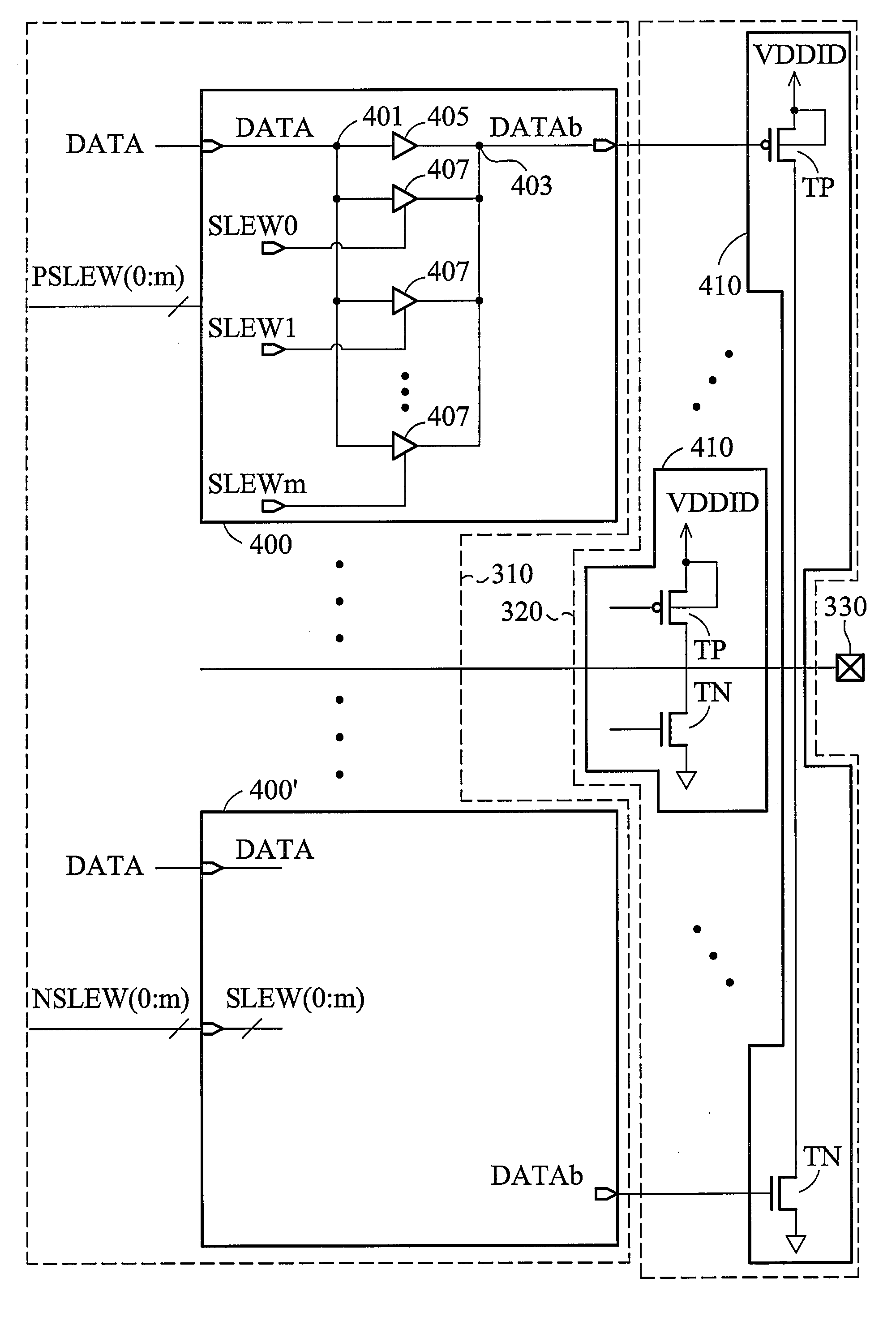
[0030]FIG. 3A is a block diagram of a slew rate controlled output buffer according to an embodiment of the invention. In FIG. 3A, the slew rate controlled output buffer 300 comprises a pre-driver circuit 310, a driver circuit 320, and a pad 330. The pre-driver circuit 310 receives an input data signal, pull-up slew rate control signals PSLEW, and pull-down slew rate control signals NSLEW. The driver circuit 320 is coupled to the pre-driver circuit 310 and driven by an output signal thereof. The pad 330 is coupled to the driver circuit 320 and driven by an output signal thereof. The pre-driver circuit 310 adjusts a slew rate of the output signal of the driver circuit 32...


PUM


Abstract

A slew rate controlled output buffer. The slew rate controlled output buffer comprises a pre-driver circuit having a data input node and a data output node and a driver circuit coupled to the output node of the pre-driver circuit. The pre-driver circuit comprises a plurality of inverters connected in parallel, each having an input terminal coupled to the input node and an output terminal coupled to the output node, wherein at least one of the inverters is selectively disabled by a slew rate control signal via a slew rate controller. The driver circuit is driven by an output signal of the pre-driver circuit.

Description

[0001]This application claims the benefit of U.S. Provisional Application No. 60 / 864,166, filed on Nov. 3, 2006, which is incorporated herein by reference.BACKGROUND OF THE INVENTION[0002]1. Field of the Invention[0003]The invention relates to semiconductor integrated circuits and, in particular, to a slew rate controlled circuit in semiconductor integrated circuit.[0004]2. Description of the Related Art[0005]An output buffer of a semiconductor device drives internal signals via an output terminal. A slew rate of an output buffer represents how quickly a voltage level of an output signal changes from one data state to another. A rate of voltage change is defined as slew rate of an output buffer.[0006]The slew rate of a driver is usually controlled by adjusting a pre-driver circuit. The pre-driver is a circuit between the core circuits and a final output driver and adjusts the timing and the driving capability to the final I / O output stage such that required I / O specifications are me...

Claims


Application Information

Patent Timeline
Patent Type & Authority Applications(United States)
IPC IPC(8): H03K19/00H03K19/0185
CPCH03K19/00361H03K17/164
Inventor JAO, CHE-YUAN
Owner MEDIATEK INC
Why Eureka
Try Eureka