Semiconductor chip package and method and system for testing the same

a technology of semiconductors and chips, applied in the field of semiconductor chip packages and a method and system for testing the same, can solve the problems of increasing test time and test costs, and achieve the effect of short time and low cos

Inactive Publication Date: 2008-05-08
SAMSUNG ELECTRONICS CO LTD
View PDF2 Cites 15 Cited by
  • Summary
  • Abstract
  • Description
  • Claims
  • Application Information

AI Technical Summary

Benefits of technology

[0011]Some embodiments provide a semiconductor chip package having a plurality of flash memory portions or having a flash memory portion and at least one heterogeneous memory portions, which can be tested at a low cost and in a short time.

Problems solved by technology

Therefore, as more memory chips are mounted on the MCP 10 and the storage capacity of each memory chip is further increased, the conventional burn-in test leads to an increase in test time and test costs, which becomes a main cause in delayed shipments of products.

Method used


Image

  • Semiconductor chip package and method and system for testing the same
  • Semiconductor chip package and method and system for testing the same
  • Semiconductor chip package and method and system for testing the same

Examples


Embodiment Construction

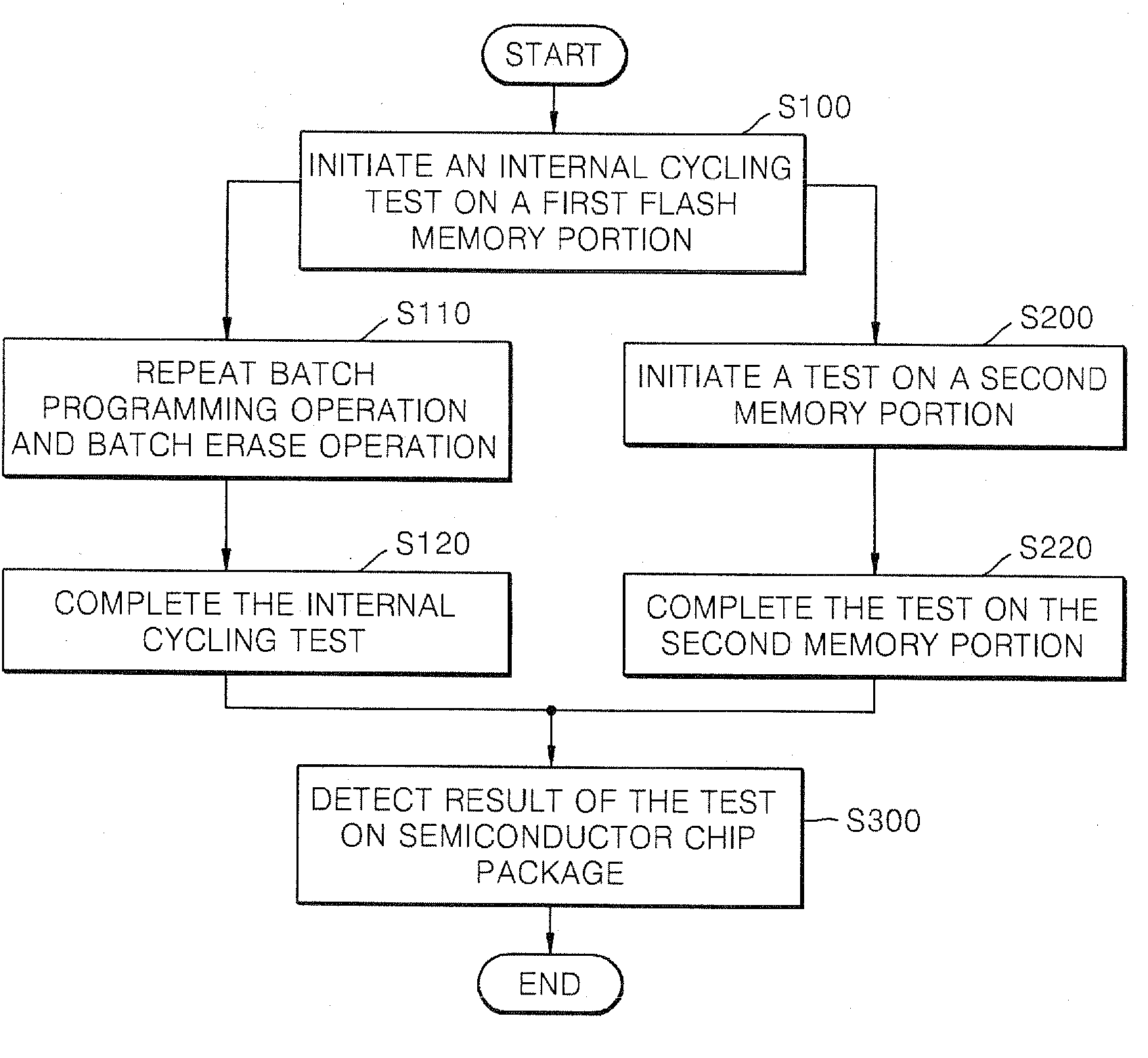
[0028]Inventive principles will now be described more fully with reference to the accompanying drawings, in which example embodiments are shown. The inventive principles may, however, be embodied in many different forms and should not be construed as being limited to the embodiments set forth herein; rather, these embodiments are provided so that this disclosure will be thorough and complete, and will fully convey the concept of the invention to those skilled in the art. The term “and / or” as used herein refers to and encompasses any and all combinations of one or more of the associated listed items.

[0029]Also, though terms like a first and a second are used to describe various members, components, regions, layers, and / or portions in various embodiments of the present invention, the members, components, regions, layers, and / or portions are not limited to these terms. These terms are used only to differentiate one member, component, region, layer, or portion from another. Therefore, a...


PUM


Abstract

A semiconductor chip package with a flash memory portion and a method and system for testing the same are provided. After an internal cycling test is automatically and independently initiated on the flash memory chip, a test on other memory portions in the semiconductor chip package is performed. The semiconductor chip package includes a first flash memory portion, at least one second memory portions, and an internal cycling tester repetitively performing a batch programming operation and a batch erase operation on the first flash memory portion.

Description

CROSS-REFERENCE TO RELATED APPLICATIONS[0001]This application claims the benefit of Korean Patent Application No. 10-2006-0107944, filed on Nov. 02, 2006, in the Korean Intellectual Property Office, the disclosure of which is incorporated herein in its entirety by reference.BACKGROUND[0002]1. Technical Field[0003]This disclosure relates to a semiconductor chip package and a method and system for testing the same, and more particularly, to a semiconductor chip package having a plurality of flash memory portions or having a flash memory portion and a heterogeneous memory portion, and a method and system for testing the same.[0004]2. Description of the Related Art[0005]Advanced electronic engineering and semiconductor integration technologies promote the miniaturization and multifunctionality of electronic products. As one example, portable terminals such as cellular phones provide a multimedia play function as well as an inherent mobile communication function. The miniaturization and ...

Claims


Application Information

Patent Timeline
Patent Type & Authority Applications(United States)
IPC IPC(8): G11C29/00
CPCG11C2029/2602G11C29/16G01R31/3183G01R31/28G01R31/3187
Inventor KWON, KI-ROCKLEE, SANG-HO
Owner SAMSUNG ELECTRONICS CO LTD
Why Eureka
Try Eureka