METHOD FOR HETEROEPITAXIAL GROWTH OF HIGH-QUALITY N-FACE GaN, InN, AND AlN AND THEIR ALLOYS BY METAL ORGANIC CHEMICAL VAPOR DEPOSITION

a technology of nitride and heteroepitaxial growth, which is applied in the growth process of polycrystalline materials, crystal growth processes, and chemically reactive gases, etc., can solve the problems of low resistance p-type (al,ga,in)n:mg films, high composition growth of high quality ingan, and the like. to achieve the effect of enhancing the charge transport properties of a nitride devi

Active Publication Date: 2008-05-15
RGT UNIV OF CALIFORNIA
View PDF95 Cites 57 Cited by
  • Summary
  • Abstract
  • Description
  • Claims
  • Application Information

AI Technical Summary

Benefits of technology

[0020]Another method for enhancing charge transport properties of a nitride device in accordance with the present invention comprises fabricating the nitride device using N-face nitride layers grown on a substrate having a growth surface with a misorientation angle between 0.5 and 10 degrees relative to a miller indexed crystallographic plane [h, i, k, l] of the substrate, where h, i, k, l are miller indices, and aligning a channel of the nitride device substantially perpendicular to a misorientation direction of the misoriented (Al, Ga, In)N epitaxial layer, wherein charge transport properties are enhanced perpendicular to the misorientation direction.

Problems solved by technology

Films and heterostructures of the opposite polarity (N-polar group-III nitride films and heterostructures) have been much less investigated due to difficulties in their growth.
One of the major challenges to III-Nitride based light emitters is the growth of high quality InGaN with high In composition.
The use of the Gallium (Ga)-face for devices limits the temperature at which the InGaN can be grown, which limits the types of devices that can be made.
Another challenge is the growth of low resistance p-type (Al,Ga,In)N:Mg films due to polarity conversion from Ga-face to N-face at high Mg doping levels.

Method used


Image

  • METHOD FOR HETEROEPITAXIAL GROWTH OF HIGH-QUALITY N-FACE GaN, InN, AND AlN AND THEIR ALLOYS BY METAL ORGANIC CHEMICAL VAPOR DEPOSITION
  • METHOD FOR HETEROEPITAXIAL GROWTH OF HIGH-QUALITY N-FACE GaN, InN, AND AlN AND THEIR ALLOYS BY METAL ORGANIC CHEMICAL VAPOR DEPOSITION
  • METHOD FOR HETEROEPITAXIAL GROWTH OF HIGH-QUALITY N-FACE GaN, InN, AND AlN AND THEIR ALLOYS BY METAL ORGANIC CHEMICAL VAPOR DEPOSITION

Examples


Embodiment Construction

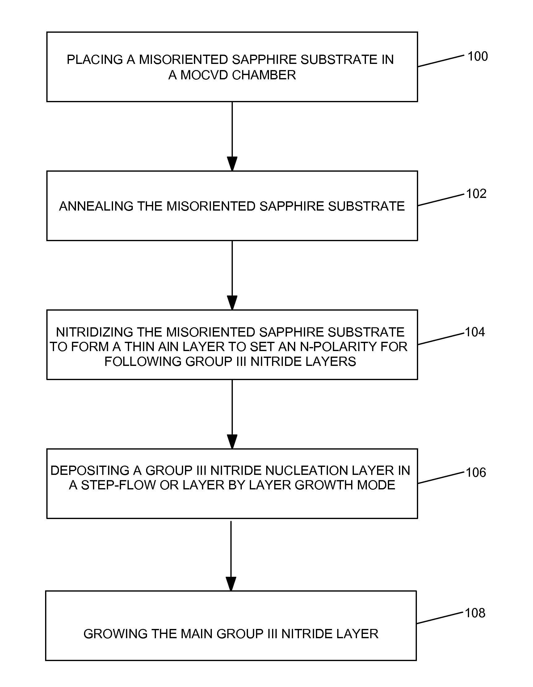
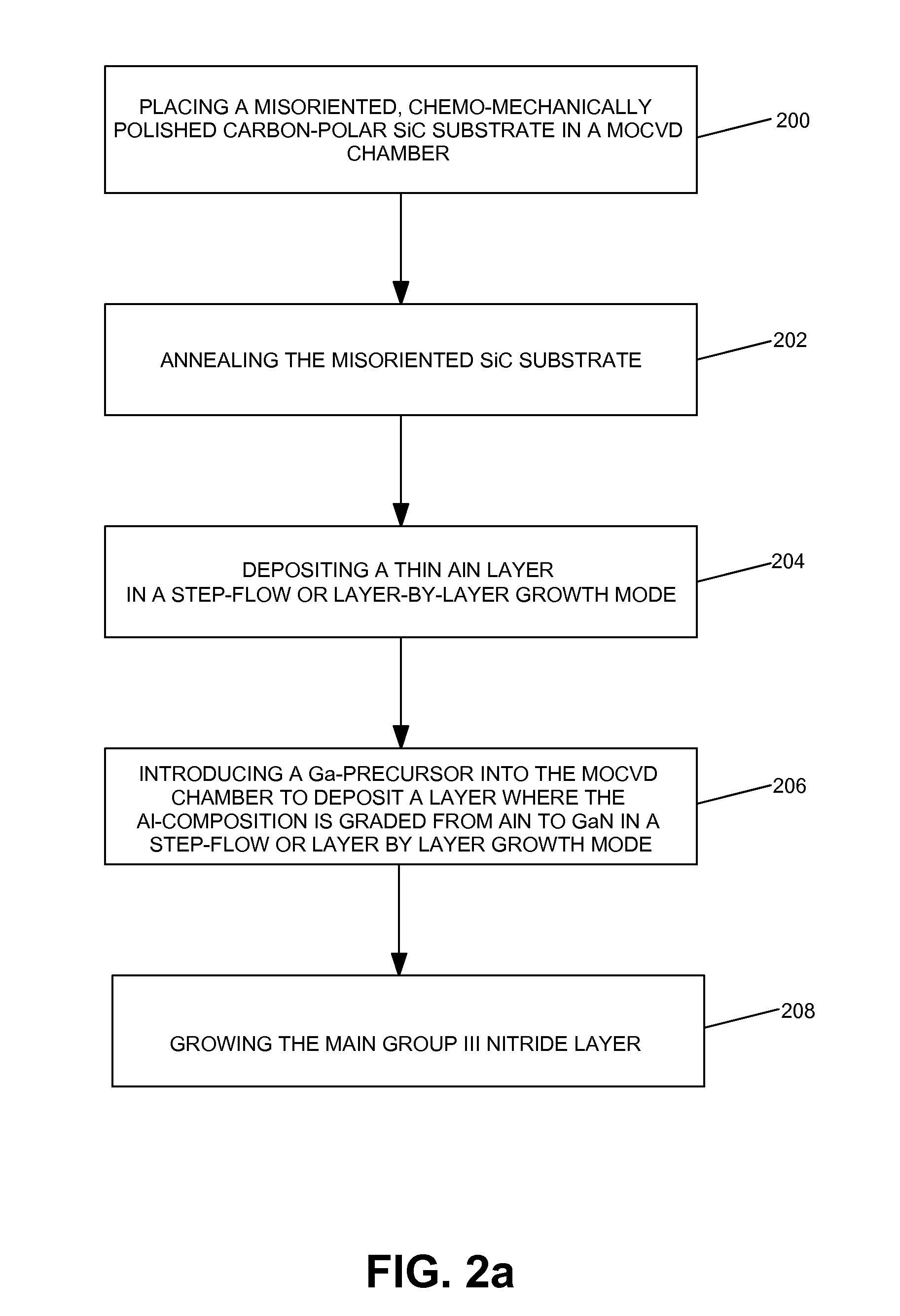
[0035]In the following description of the preferred embodiment, reference is made to the accompanying drawings which form a part hereof, and in which is shown by way of illustration a specific embodiment in which the invention may be practiced. It is to be understood that other embodiments may be utilized and structural changes may be made without departing from the scope of the present invention.

[0036]Overview

[0037]This invention will allow for the creation of transistors that cannot be fabricated on traditional Ga-polar GaN. The present invention will also allow novel polarization-based band structure designs to create more efficient LEDs and LDs. The reverse polarization fields in N-polar heterostructures, in comparison to Ga-polar heterostructures, result in lower operating voltages, shrink the width of the depletion region of the p-n-junction, and improve carrier injection, leading to advances in device performance. Deposition on N-polar surfaces enables the growth of InGaN wit...


PUM

PropertyMeasurementUnit
misorientation angleaaaaaaaaaa
thickaaaaaaaaaa

Abstract

Methods for the heteroepitaxial growth of smooth, high quality films of N-face GaN film grown by MOCVD are disclosed. Use of a misoriented substrate and possibly nitridizing the substrate allow for the growth of smooth N-face GaN and other Group III nitride films as disclosed herein. The present invention also avoids the typical large (μm sized) hexagonal features which make N-face GaN material unacceptable for device applications. The present invention allows for the growth of smooth, high quality films which makes the development of N-face devices possible.

Description

CROSS-REFERENCE TO RELATED APPLICATIONS[0001]This application claims the benefit under 35 U.S.C. Section 119(e) of the following co-pending and commonly-assigned U.S. patent application: U.S. Provisional Application Ser. No. 60 / 866,035 filed on Nov. 15, 2006, by Stacia Keller, Umesh K. Mishra and Nicholas A. Fichtenbaum, entitled “METHOD FOR HETEROEPITAXIAL GROWTH OF HIGH-QUALITY N-FACE GaN, InN, AND AlN AND THEIR ALLOYS BY METAL ORGANIC CHEMICAL VAPOR DEPOSITION,” attorneys' docket number 30794.207-US-P1 (2007-121-1);[0002]which application is incorporated by reference herein.[0003]This application is related to the following co-pending and commonly-assigned applications:[0004]U.S. patent application Ser. No. 11 / 523,286, filed on Sep. 18, 2006, by Siddharth Rajan, Chang Soo Suh, James S. Speck, and Umesh K. Mishra, entitled “N-POLAR ALUMINUM GALLIUM NITRIDE / GALLIUM NITRIDE ENHANCEMENT-MODE FIELD EFFECT TRANSISTOR”, attorney's docket number 30794.148-US-U1 (2006-107-2), which claims...

Claims


Application Information

Patent Timeline
Patent Type & Authority Applications(United States)
IPC IPC(8): H01L21/36
CPCH01L21/02378H01L21/02433H01L21/02381H01L21/0242C30B25/02H01L21/02458H01L21/0257H01L21/0237H01L21/0262H01L21/0254C30B29/403
Inventor KELLER, STACIAMISHRA, UMESH KUMARFICHTENBAUM, NICHOLAS A.
Owner RGT UNIV OF CALIFORNIA
Why Eureka
Try Eureka