

Light-emitting diode with luminescent charge transport layer
a technology of charge transport layer and light-emitting diodes, which is applied in the direction of discharge tube luminescnet screens, discharge tube/lamp details, electric discharge lamps, etc., can solve the problems of catastrophic failure of devices and significant number of short-circuits, and achieve low short-circuit risk, low voltage drop across the charge transport layer, and high thickness
- Summary
- Abstract
- Description
- Claims
- Application Information
AI Technical Summary
Benefits of technology
Problems solved by technology
Method used
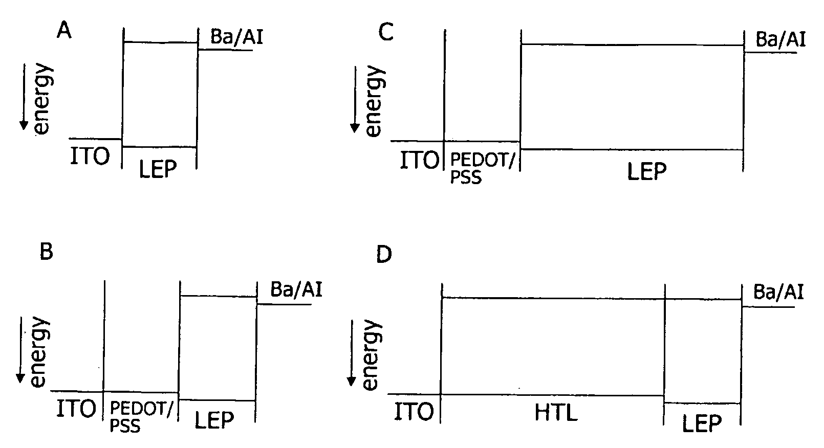
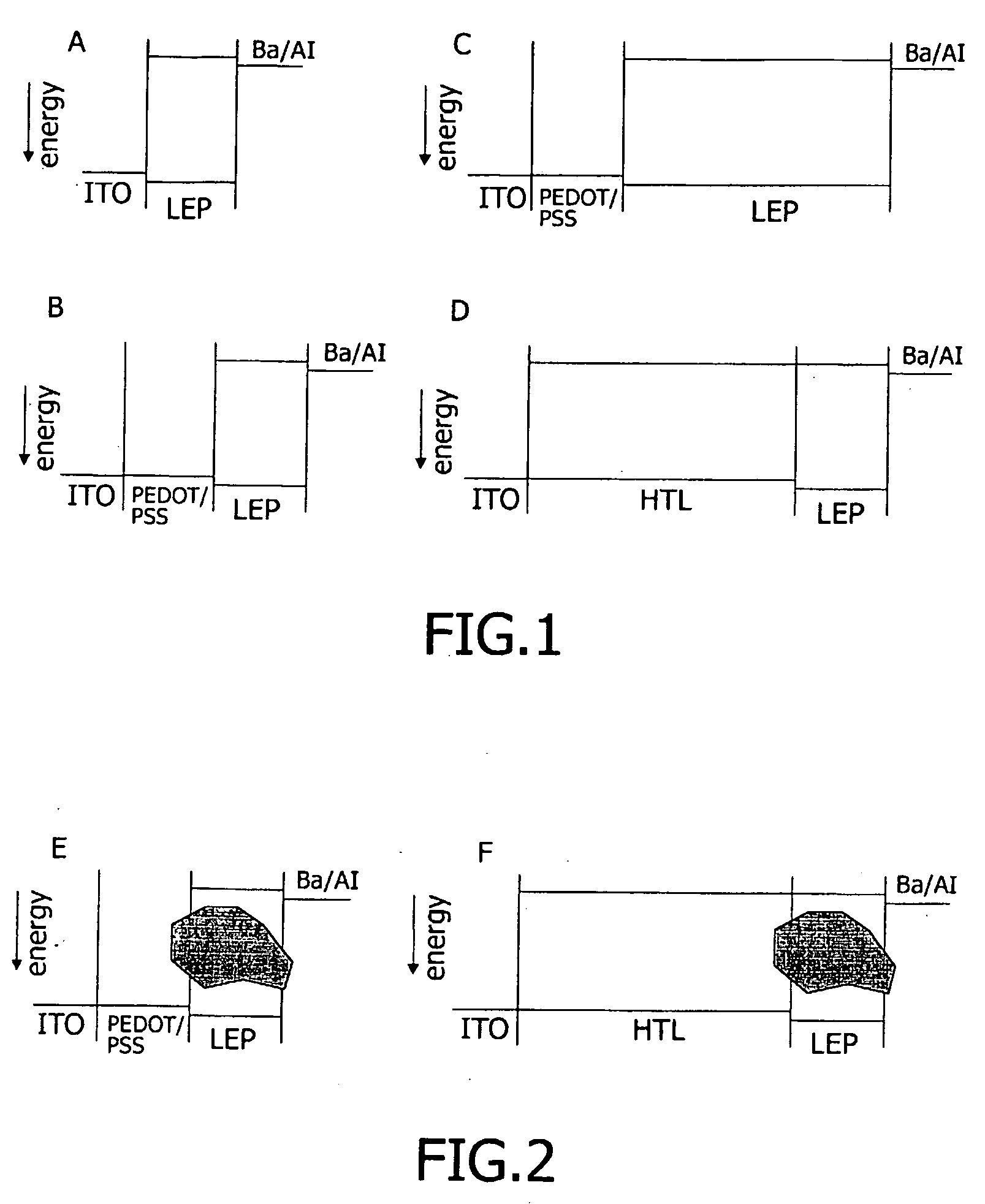
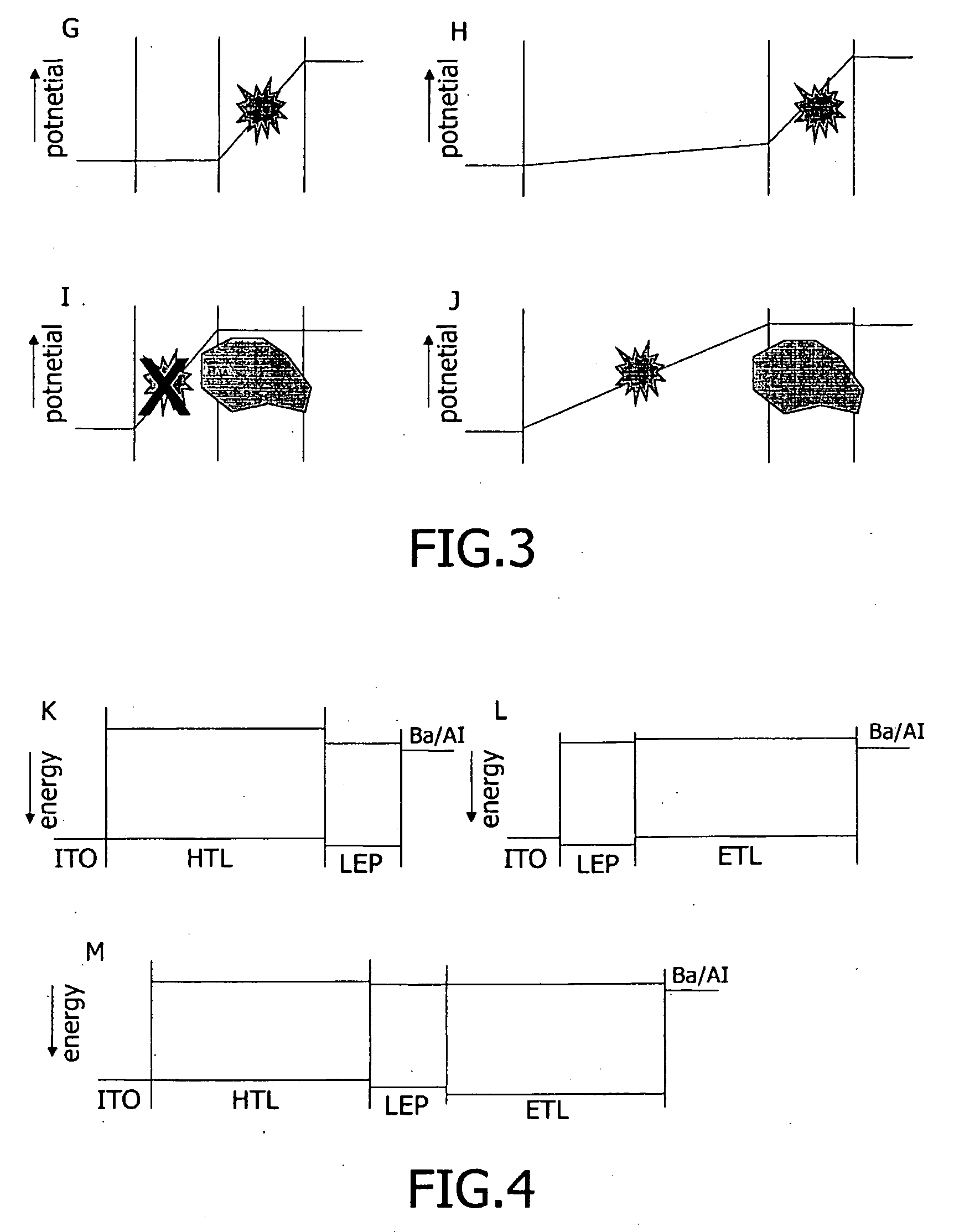
Image

Examples
Embodiment Construction
[0040]Polymer synthesis: MEH-PPV, BEH-PPV, and BEH / BB-PPV 1 / 3 were synthesized by the MEH-PPV method in the presence of 0.5-1.0% of 4-methoxyphenol, cf. Neef et al. in Macromolecules 2000, 33, 2311. The structures of the polymers used are shown below. The precursors were carefully purified by crystallisation (3×) and the obtained polymers were purified by a second precipitation from acetone. NRS-PPV was synthesized in accordance with the procedure indicated in Adv. Mater. 1998, 10, 1340:
[0041]Polymer analysis: Molecular weights were determined by gel permeation chromatography (GPC); they were measured in trichlorobenzene at 135° C. and calibrated with polystyrene standards.
[0042]The combination of BEH-PPV and BB-PPV in various ratios in copolymers can induce a variation from insoluble in toluene (pure BB-PPV) to highly soluble in toluene (pure BEH-PPV), depending on the amount of BB-PPV in the copolymer. The solubility in toluene of BEH / BB-PPV in various ratios 1:x (x=1-3) drops fro...
PUM
| Property | Measurement | Unit |
|---|---|---|
| thick | aaaaa | aaaaa |
| thickness | aaaaa | aaaaa |
| thickness | aaaaa | aaaaa |
Abstract
Description
Claims
Application Information