Flip Chip Assembly Having Improved Thermal Dissipation

a technology of flip chip and heat dissipation, which is applied in the manufacture of printed circuits, printed circuit aspects, basic electric elements, etc., can solve the problems of only placing the flip chip, insufficient thermal pathways to obtain the desired heat flow, and limited primary heat paths, so as to improve the design of the flip chip and the circuit substrate, and enhance the heat dissipation effect of the flip chip

Active Publication Date: 2008-05-22
BELL SEMICON LLC
View PDF23 Cites 57 Cited by
  • Summary
  • Abstract
  • Description
  • Claims
  • Application Information

AI Technical Summary

Benefits of technology

[0009]The present invention addresses the above-identified need by providing improved flip chip and circuit substrate designs. Advantageously, embodiments of these designs enhance heat dissipation from the flip chip when compared to conventional designs.
[0012]In an illustrative embodiment, an assembly comprises a stiffener, a circuit substrate and an IC chip. The circuit substrate is shaped such that it defines an aperture over the stiffener. The IC chip is attached to several signal solder bumps and thermal solder bumps. The signal solder bumps serve to electrically couple the IC chip to the circuit substrate. The thermal solder bumps are metallurgically bonded to the IC chip and that region of the stiffener revealed by the aperture in the circuit substrate. Advantageously, the thermal solder bumps provide an efficient thermal conductivity pathway between the IC chip and the stiffener. Cooling of the IC chip is thereby enhanced by using an assembly in accordance with aspects of the invention.

Problems solved by technology

In many flip chip designs however, solder bumps are only placed along the periphery of the IC chip.
As a result, this primary heat path is limited by the cumulative cross sectional area of the solder bumps and the low thermal conductivity of the non-electrically conductive materials comprising the circuit substrate.
Consequently, these thermal pathways are often inadequate to obtain a desired heat flow.
When heat flow from the IC chip to the stiffener is inadequate, the IC chip's functionality and / or speed must be limited so that the IC chip does not exceed a temperature at which its lifetime is adversely affected.
Unfortunately, these attempts typically result in only small improvements to the heat flow from the flip chip.
While effective at increasing the heat flow from the flip chip, this solution results in added cost and may not be possible due to space constraints.

Method used


Image

  • Flip Chip Assembly Having Improved Thermal Dissipation
  • Flip Chip Assembly Having Improved Thermal Dissipation
  • Flip Chip Assembly Having Improved Thermal Dissipation

Examples


Embodiment Construction

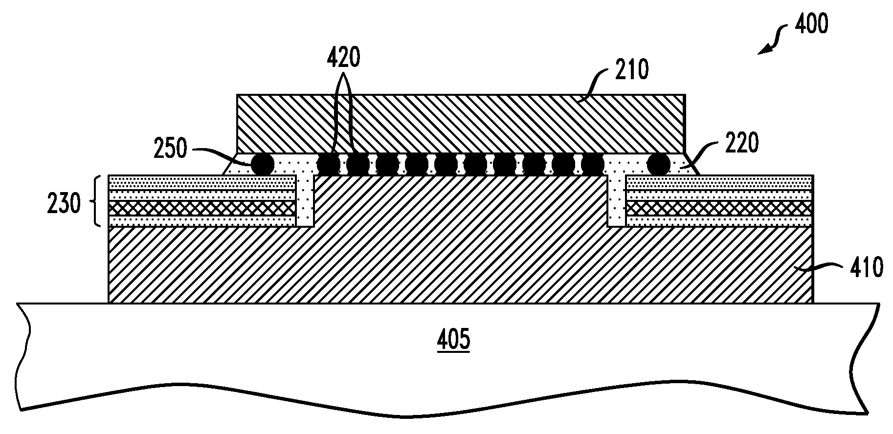
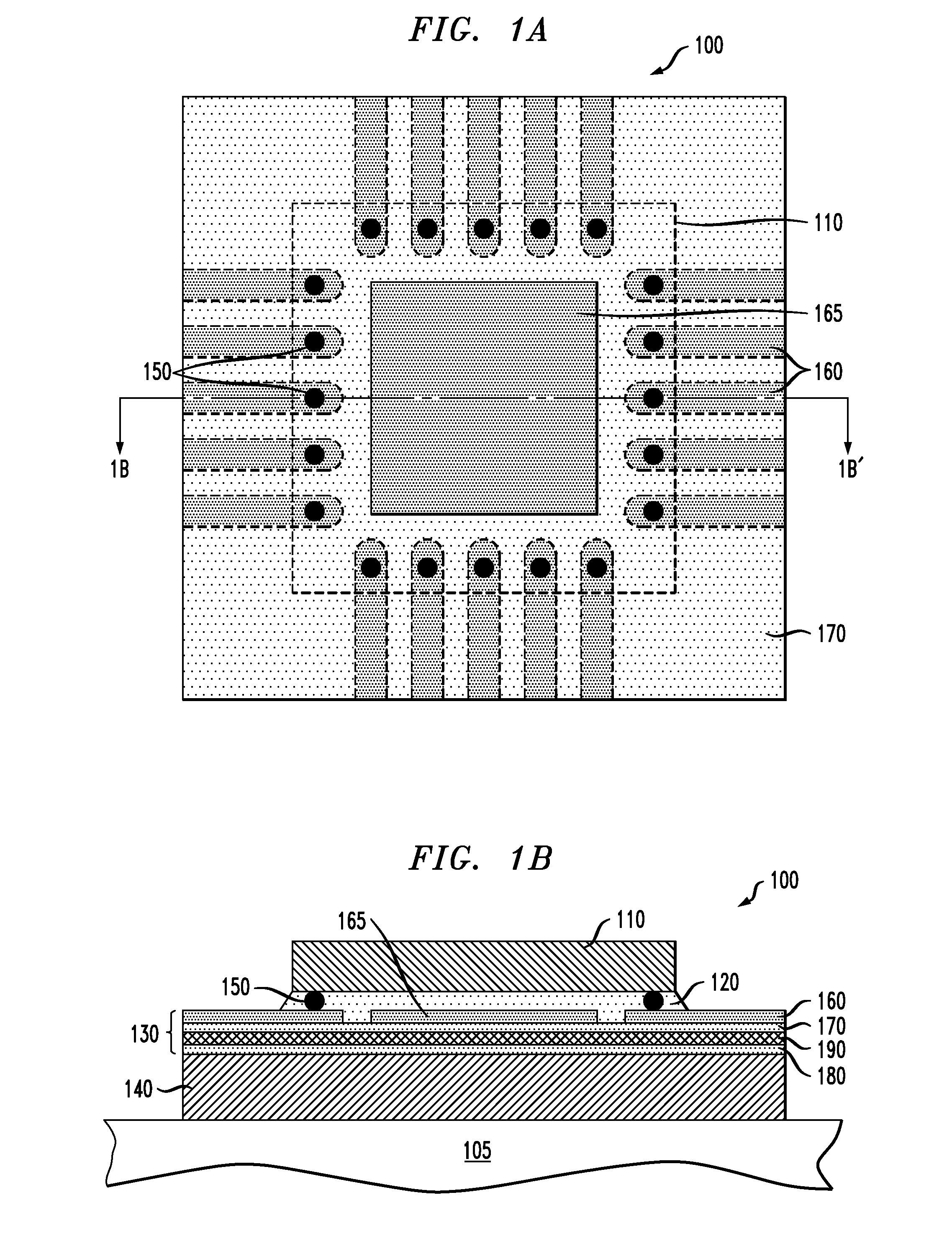
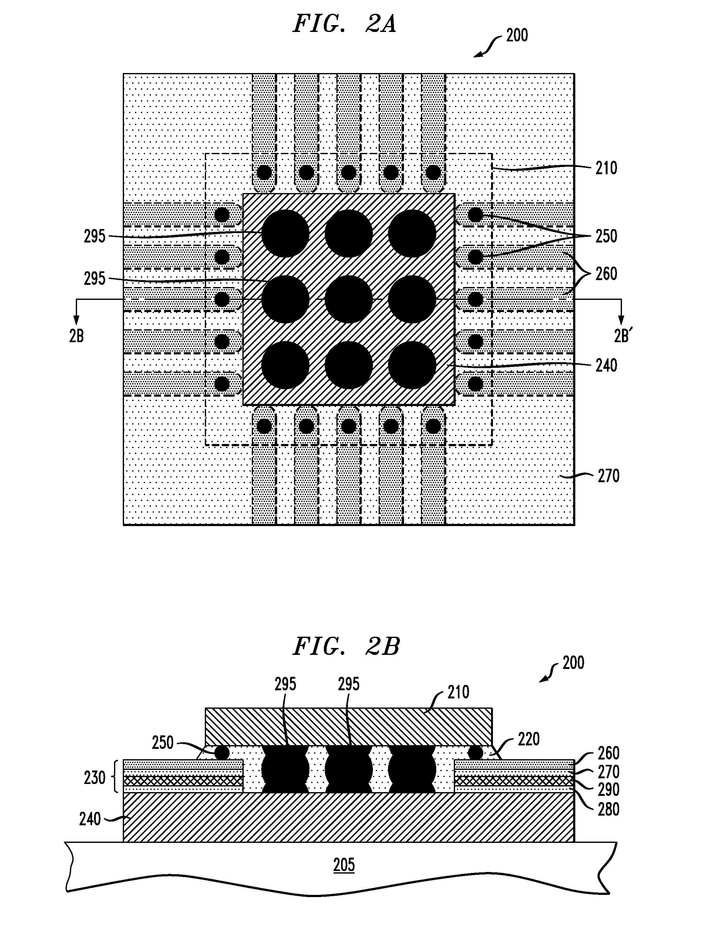
[0021]This invention will be illustrated herein in conjunction with exemplary assemblies comprising flip chips and circuit substrates. It should be understood, however, that the invention is not limited to the particular arrangements, materials, structures and processing steps shown and described herein. Modifications to the illustrative embodiments coming within the scope of this invention will become apparent to those skilled in the art from the following description.

[0022]It should also be understood that the various elements shown in the accompanying figures are not drawn to scale. Moreover, for economy of description, the figures are restricted to only those regions of the exemplary assemblies that aid in showing aspects of the invention. For example, in actual application, a circuit substrate in accordance with aspects of the invention will likely be more extensive than those circuit substrates illustrated herein. However, these more extensive circuit substrates will still com...


PUM


Abstract

An assembly comprises a stiffener, a circuit substrate and an IC chip. The stiffener has a surface with a first region and a second region. The circuit substrate covers at least a portion of the first region of the stiffener, while the IC chip overlies at least a portion of each of the first and second regions of the stiffener. The assembly further comprises a signal solder bump and a thermally conductive feature. The signal solder bump contacts the IC chip and the circuit substrate. The thermally conductive feature is disposed between, and is metallurgically bonded to, the integrated circuit chip and the second region of the stiffener. The thermally conductive feature provides an efficient thermal conductivity pathway between the IC chip and the stiffener.

Description

CROSS REFERENCE TO RELATED APPLICATIONS[0001]Related patent applications are U.S. patent application Ser. No. 11 / 375,302, entitled “Low Thermal Resistance Assembly for Flip-Chip Applications,” and International Application No. PCT / US2004 / 033982, entitled “Printed Circuit Board Assembly Having Improved Thermal Energy Dissipation,” both commonly assigned herewith and incorporated by reference herein.FIELD OF THE INVENTION[0002]This invention relates generally to integrated circuit chips, and, more particularly, to flip chips and circuit substrates.BACKGROUND OF THE INVENTION[0003]Direct chip attachment (DCA) refers to a semiconductor assembly technology wherein an integrated circuit (IC) chip is directly mounted on and electrically connected to its final circuit substrate instead of undergoing traditional assembly and packaging. The elimination of conventional device packaging in DCA both simplifies the manufacturing process and reduces the space that the IC chip occupies on the final...

Claims


Application Information

Patent Timeline
Patent Type & Authority Applications(United States)
IPC IPC(8): H01L23/34
CPCH01L21/563H01L2224/73204H01L23/3677H01L24/17H01L2224/0401H01L2224/0603H01L2224/13099H01L2224/1403H01L2224/16H01L2224/32188H01L2924/01013H01L2924/01029H01L2924/0103H01L2924/01049H01L2924/01074H01L2924/01078H01L2924/01079H01L2924/01082H01L2924/14H05K1/0204H05K3/0061H05K3/3436H05K2201/09054H05K2201/10674H05K2203/041H01L2924/01006H01L2924/01019H01L2924/01023H01L2924/01033H01L2924/01047H01L2924/014H01L2224/1703H01L2224/73203H01L23/13H01L2924/00013H01L2924/00012H01L2224/29099H01L24/16H01L2224/05124H01L2224/05155H01L2224/05647H01L2224/0615H01L2224/14H01L2924/00014H01L2924/013
Inventor AMIN, AHMEDCROUTHAMEL, DAVID L.OSENBACH, JOHN W.SHILLING, THOMAS H.VACCARO, BRIAN T.
Owner BELL SEMICON LLC
Why Eureka
Try Eureka