Three dimensional integrated passive device and method of fabrication

a passive device and three-dimensional technology, applied in the field of three-dimensional integrated passive devices and methods of fabrication, electronic devices, can solve the problems of increasing the overall device footprint, device footprint and cos

Inactive Publication Date: 2008-05-29
NORTH STAR INNOVATIONS
View PDF14 Cites 63 Cited by
  • Summary
  • Abstract
  • Description
  • Claims
  • Application Information

AI Technical Summary

Problems solved by technology

Consequently, these passive components can occupy a large portion of the circuit board area and commensurately contribute to a large share of product assembly costs.
In conventional applications, a harmonic filter and an RF coupler are two distinct components, each of which adds to the overall device footprint.
Yet challenges remain in the further reduction of the device footprint and cost while concurrently simplifying fabrication processes and providing effective coupling and directionality.
However, again challenges remain in further reducing the device footprint relative to the footprint achieved utilizing two-dimensional integration of integrated passive devices and MEMS components, reducing cost, and simplifying fabrication processes.

Method used


Image

  • Three dimensional integrated passive device and method of fabrication
  • Three dimensional integrated passive device and method of fabrication
  • Three dimensional integrated passive device and method of fabrication

Examples


Embodiment Construction

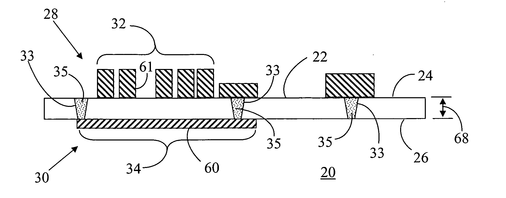
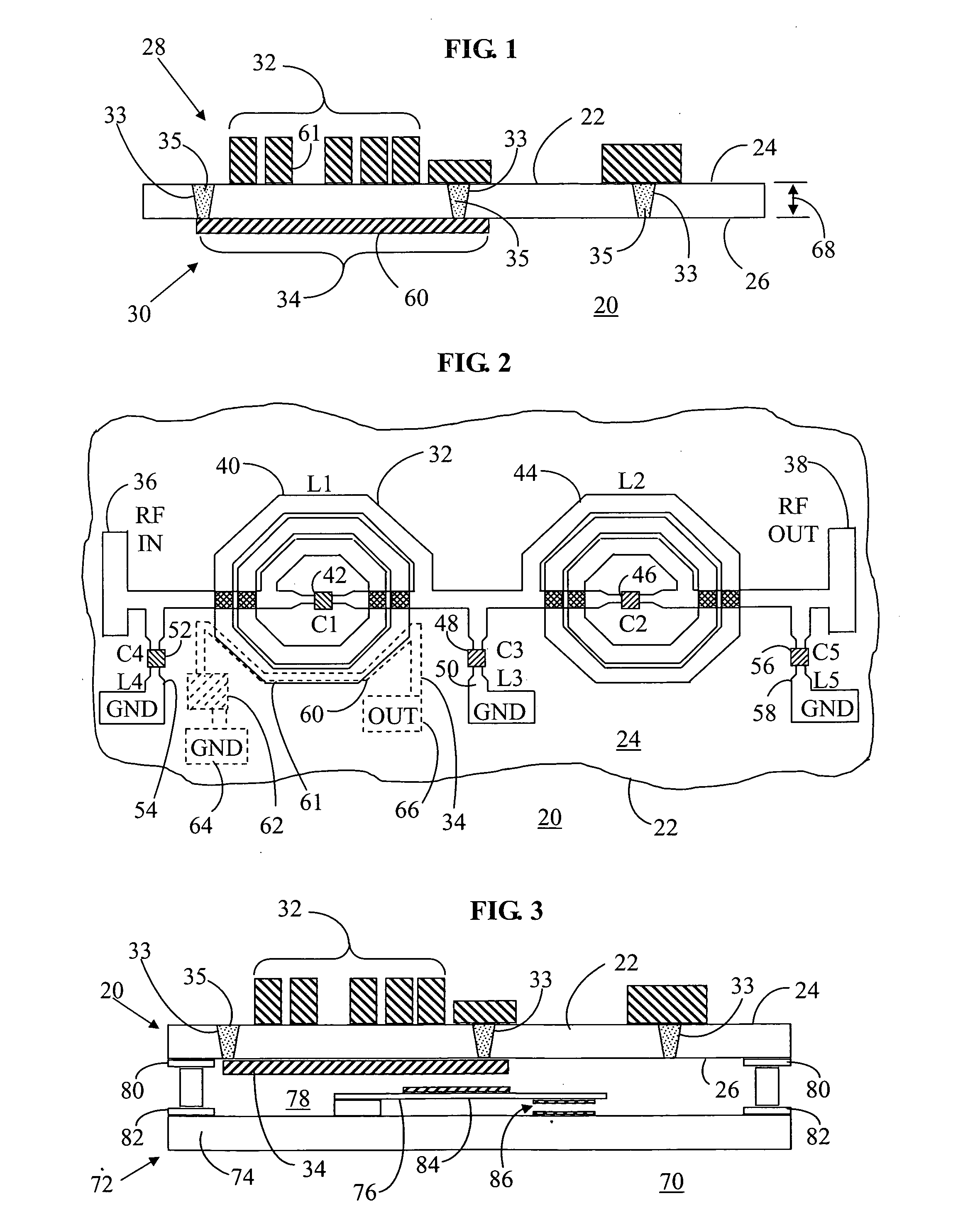
[0012]In one embodiment, an electronic device includes a three-dimensional integrated passive device. This three-dimensional integrated passive device may include, for example, a radio frequency (RF) circuit, such as a harmonic filter, integrated with an RF coupler. However, the three-dimensional integrated passive device may alternatively or additionally include other passive and active devices configured in accordance with a desired application of the electronic device.

[0013]In another embodiment, the electronic device based upon a three-dimensional integrated passive device architecture may be combined with a microelectromechanical systems (MEMS) component in a stacked fashion. The resulting combination may be utilized within an RF MEMS-based reconfigurable front-end system for upcoming tunable RF modules that can transmit and decode numerous radio signals, e.g., Universal Mobile Telecommunications System, Time Division Multiple Access, Code Division Multiple Access, and Bluetoot...


PUM


Abstract

An integrated passive device (20) includes a first wafer (22), a first integrated device (28) formed on a first surface (24) of the wafer (22), and a second integrated device (30) formed on a second surface (26) of the wafer (22), the second surface (26) opposing the first surface (24). A microelectromechanical (MEMS) device (72) includes a second wafer (74) having a MEMS component (76) formed thereon. The integrated passive device (20) and the MEMS device (72) are coupled to form an IPD / MEMS stacked device (70) in accordance with a fabrication process (90). The fabrication process (90) calls for forming (94) the second integrated device (30) on the second surface (26) of the wafer (22), constructing (100) the MEMS component (76) on the wafer (74), coupling (104) the wafers (22, 74), then creating the first integrated device (28) on the first surface (24) of the first wafer (22).

Description

TECHNICAL FIELD [0001]The present invention relates generally to electronic devices. More specifically, the present invention relates to electronic devices fabricated using integrated passive device (IPD) technology.BACKGROUND OF THE INVENTION[0002]The explosion of growth in the portable wireless electronics industry has provided numerous challenges and opportunities for manufacturers of radio frequency (RF) components. The latest portable wireless telephony, data, and Internet access products demand greater functionality, higher performance, and lower cost in smaller and lighter formats. Additionally, wireless applications are spreading to new markets—from radar-equipped passenger vehicles to biomedical devices that, when injected or inserted, send data to a receiver outside the body. This demand has been satisfied in part by major advances in integrated circuit (IC) device technology and by the introduction of smaller packaging form factors, smaller discrete passive components, an...

Claims


Application Information

Patent Timeline
Patent Type & Authority Applications(United States)
IPC IPC(8): H01P1/00H01L21/50
CPCB81B2207/092B81B7/0077
Inventor LIU, LIANJUN
Owner NORTH STAR INNOVATIONS
Why Eureka
Try Eureka