Chip antenna

a chip antenna and antenna technology, applied in the field of chip antennas, can solve the problems of shortening the development time, reducing the number of experiments, and limiting the design of chip antennas with broadband characteristics, and achieve good standing wave ratio

Inactive Publication Date: 2008-05-29
SAMSUNG ELECTRO MECHANICS CO LTD
View PDF10 Cites 4 Cited by
  • Summary
  • Abstract
  • Description
  • Claims
  • Application Information

AI Technical Summary

Benefits of technology

[0009]An aspect of the present invention provides a chip antenna having broadband frequency characteristics and a good standing wave ratio (SWR) in a broadband frequency range.

Problems solved by technology

On the other hand, a broader bandwidth of the chip antenna decreases the number of experiments, thereby shortening development time.
However, there have been limitations in designing the chip antenna with broadband characteristics by virtue of such a feeding structure.
In addition, the chip antenna, when assembled inside the mobile telecommunication terminal, is altered in frequency characteristics, inevitably entailing a tuning process thereof.

Method used


Image

  • Chip antenna
  • Chip antenna
  • Chip antenna

Examples


Embodiment Construction

[0031]Exemplary embodiments of the present invention will now be described in detail with reference to the accompanying drawings.

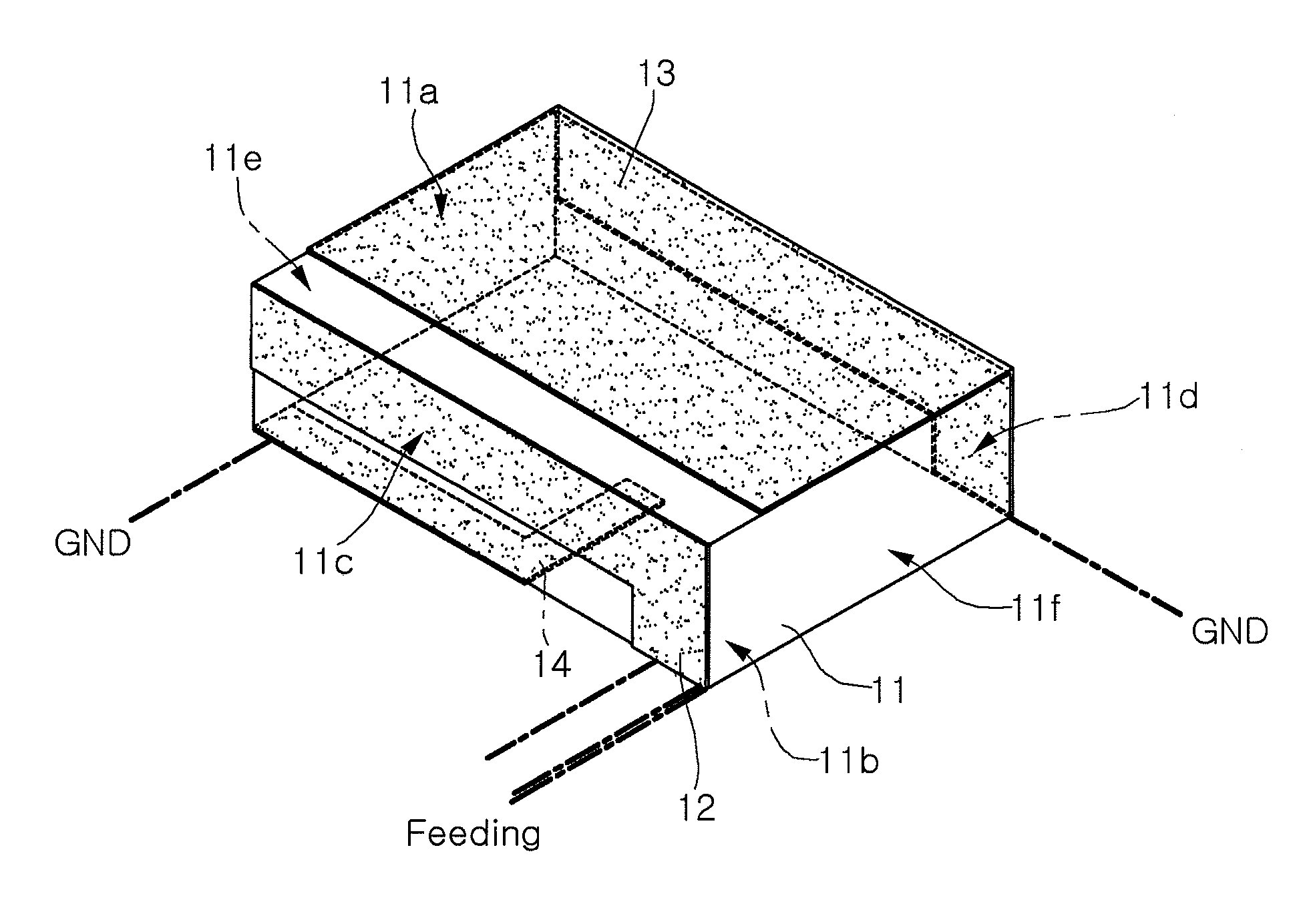
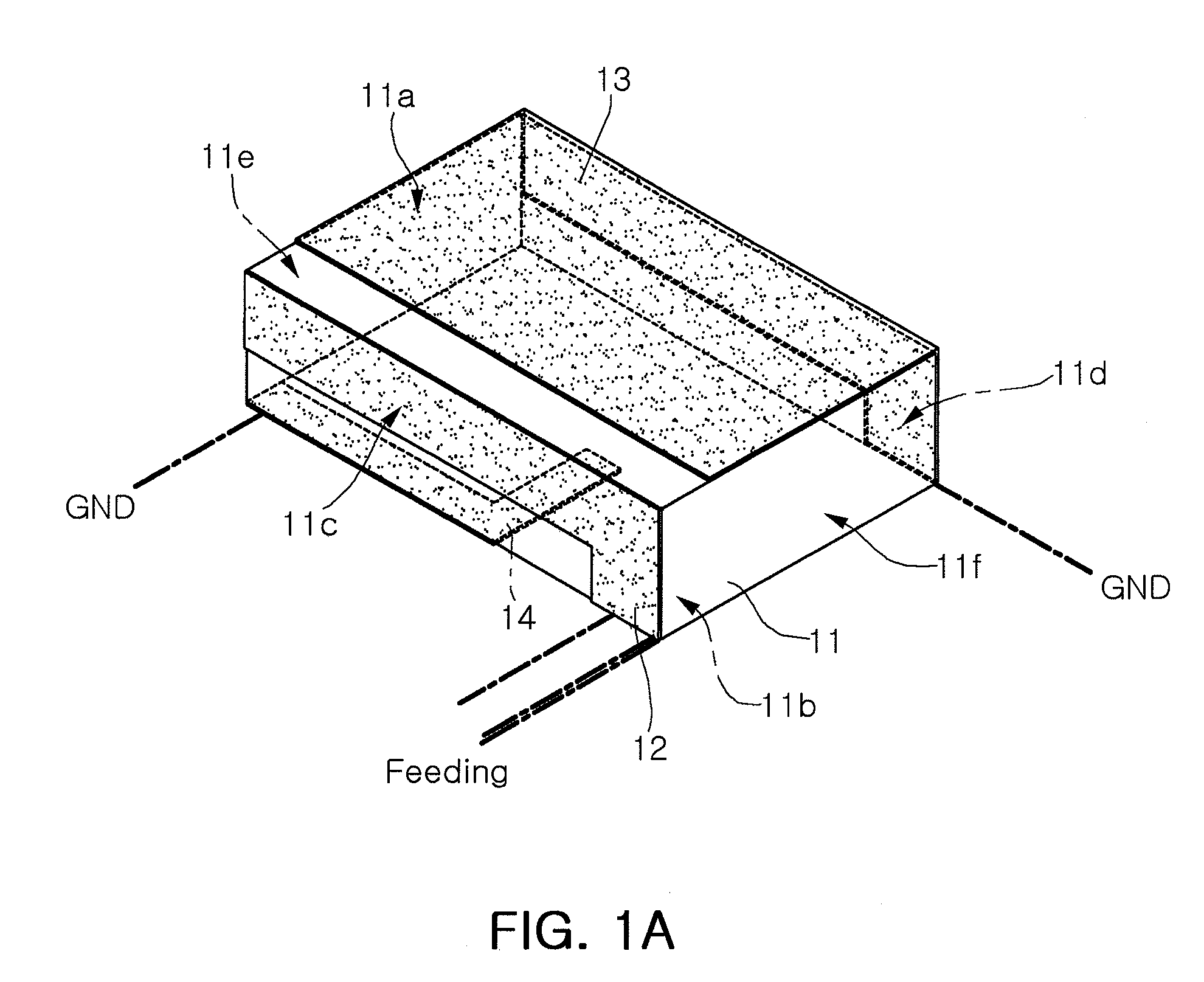
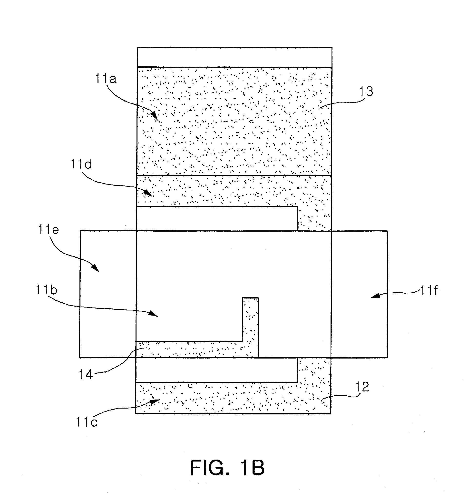
[0032]FIGS. 1A and 1B are a perspective view and a cross-sectional view illustrating a chip antenna, respectively according to an exemplary embodiment of the invention.

[0033]Referring to FIGS. 1A and 1B, the chip antenna of the present embodiment includes a dielectric block 11, a first conductive pattern 12, a second conductive pattern 13 and a third conductive pattern 14.

[0034]The dielectric block 11 may be shaped as a rectangular parallelepiped. The dielectric block 11 has a top surface 11a and a bottom surface 11b opposing each other, and first to fourth side surfaces 11c, 11d, 11e, and 11f connecting the top surface 11a and the bottom surface 11b. The bottom surface 11b of the dielectric block is brought in contact with a board when an antenna is mounted on the board.

[0035]The dielectric block 11 may be formed of a ceramic material.

[0036]A first conduc...


PUM


Abstract

There is provided a chip antenna including: a dielectric block; a first conductive pattern formed on at least one surface of the dielectric block to connect to an external feeding part; a second conductive pattern spaced apart from the first conductive pattern at a certain distance so as to be capacitively coupled to the first conductive pattern to act as a radiator, the second conductive pattern having one end connected to an external ground part; and a third conductive pattern spaced apart from the first conductive pattern at a certain distance so as to be capacitively coupled to the first conductive pattern to enable impedance matching of the antenna, the third conductive pattern having one end connected to the external ground part.

Description

CROSS-REFERENCE TO RELATED APPLICATIONS[0001]This application claims the priority of Korean Patent Application No. 2006-115951 filed on Nov. 22, 2006, in the Korean Intellectual Property Office, the disclosure of which is incorporated herein by reference.BACKGROUND PART OF THE INVENTION[0002]1. Field of the Invention[0003]The present invention relates to a chip antenna and a mobile telecommunication terminal having the same, and more particularly, to a chip antenna having a plurality of conductive patterns capacitively coupled to a conductive pattern connected to a feeding part, a mobile telecommunication terminal having the chip antenna, and a printed circuit board for use in the mobile telecommunication terminal.[0004]2. Description of the Related Art[0005]In a mobile telecommunication field, an antenna is a passive device whose characteristics are susceptible to ambient environment. The antenna is installed in a base station, or attached to a relay device or a wireless telecommun...

Claims


Application Information

Patent Timeline
Patent Type & Authority Applications(United States)
IPC IPC(8): H01Q1/50H01Q1/38H01Q9/04
CPCH01Q1/2283H01Q1/243H05K2201/10636H05K1/0243H01Q9/42Y02P70/50H01Q1/38H01Q9/0407H04B1/3833
Inventor CHANG, KI WONSEO, JEONG SIKPARK, HYUN DOSUNG, JAE SUK
Owner SAMSUNG ELECTRO MECHANICS CO LTD
Why Eureka
Try Eureka