Method of improving a surface of a semiconductor substrate

Active Publication Date: 2008-05-29
SOITEC
View PDF9 Cites 2 Cited by
  • Summary
  • Abstract
  • Description
  • Claims
  • Application Information

AI Technical Summary

Benefits of technology

[0005]The present invention now provides a method of improving a surface of a semiconductor substrate that is at least partially made of silicon, wherein defects present in or on the semiconductor substrate can be really repaired to provide a semiconductor substrate that has a high surface quality. This method comprises a deposition step comprising a selective epitaxial deposition of silicon in at least one hole on the surface of the semiconductor substrate.
[0006]The present invention makes it possible to deposit silicon in the hole(s) to seal or to close them selectively with high-quality mono-crystalline silicon material wherein the formation of polycrystalline silicon is avoided, such that the original hole disappears from the surface and the resulting repaired surface provides a high surface quality which is comparable to surfaces which are free from holes or defects from the outset.

Problems solved by technology

Deficient wafers, such as wafers or layers with holes or scratches on their surface or with oxide precipitates or so-called “HF-defects”, which are present in or on a wafer and will be apparent by an HF-etch step, are mostly not suitable for further use.
Although such methods lead, in the first instance, to a superficial improvement of the surface condition of a defective wafer by smoothing, abrasion or defect covering of the respective wafer, the known methods are mostly very laborious and the corresponding defects cannot really be repaired.

Method used


Image

  • Method of improving a surface of a semiconductor substrate
  • Method of improving a surface of a semiconductor substrate
  • Method of improving a surface of a semiconductor substrate

Examples


Embodiment Construction

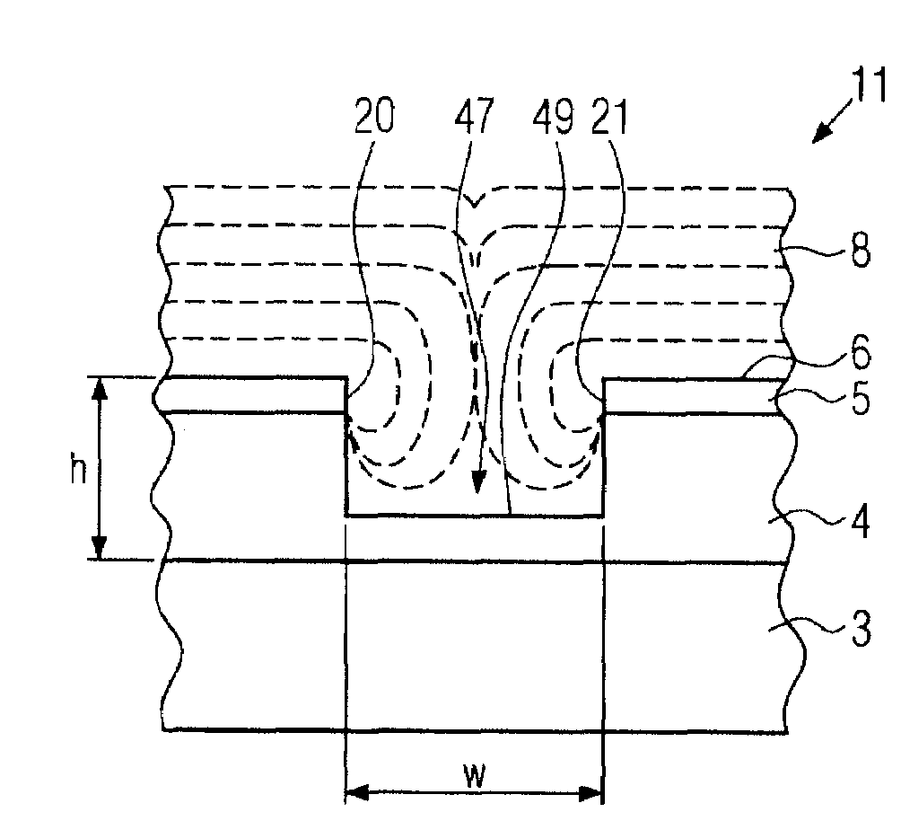
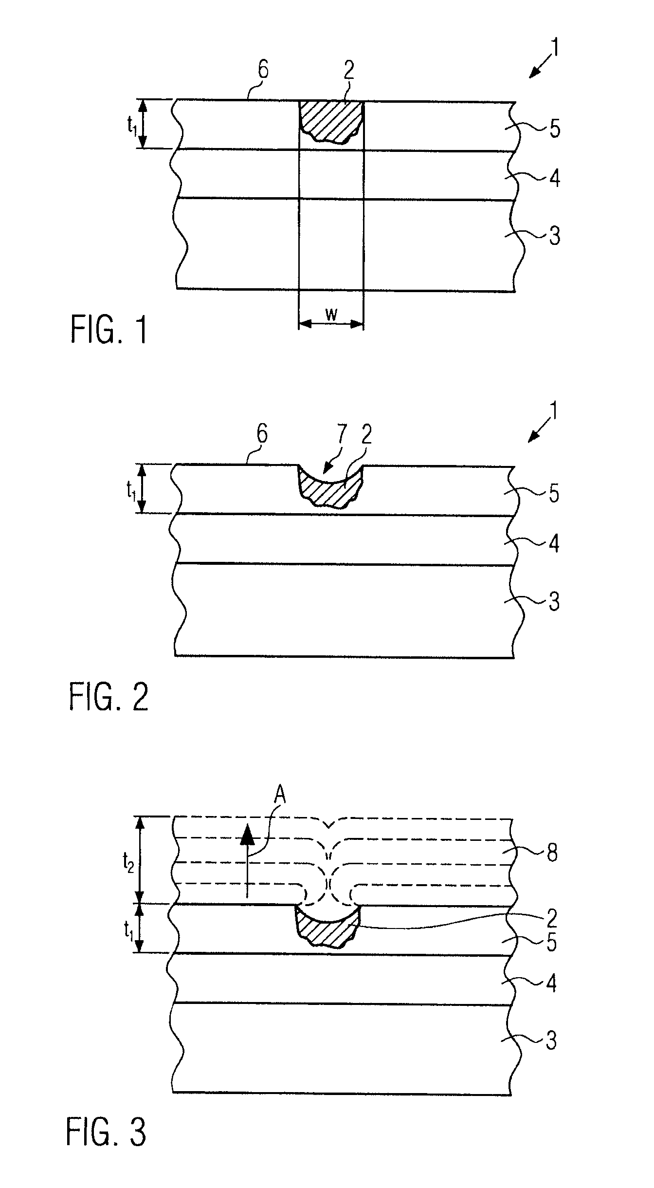
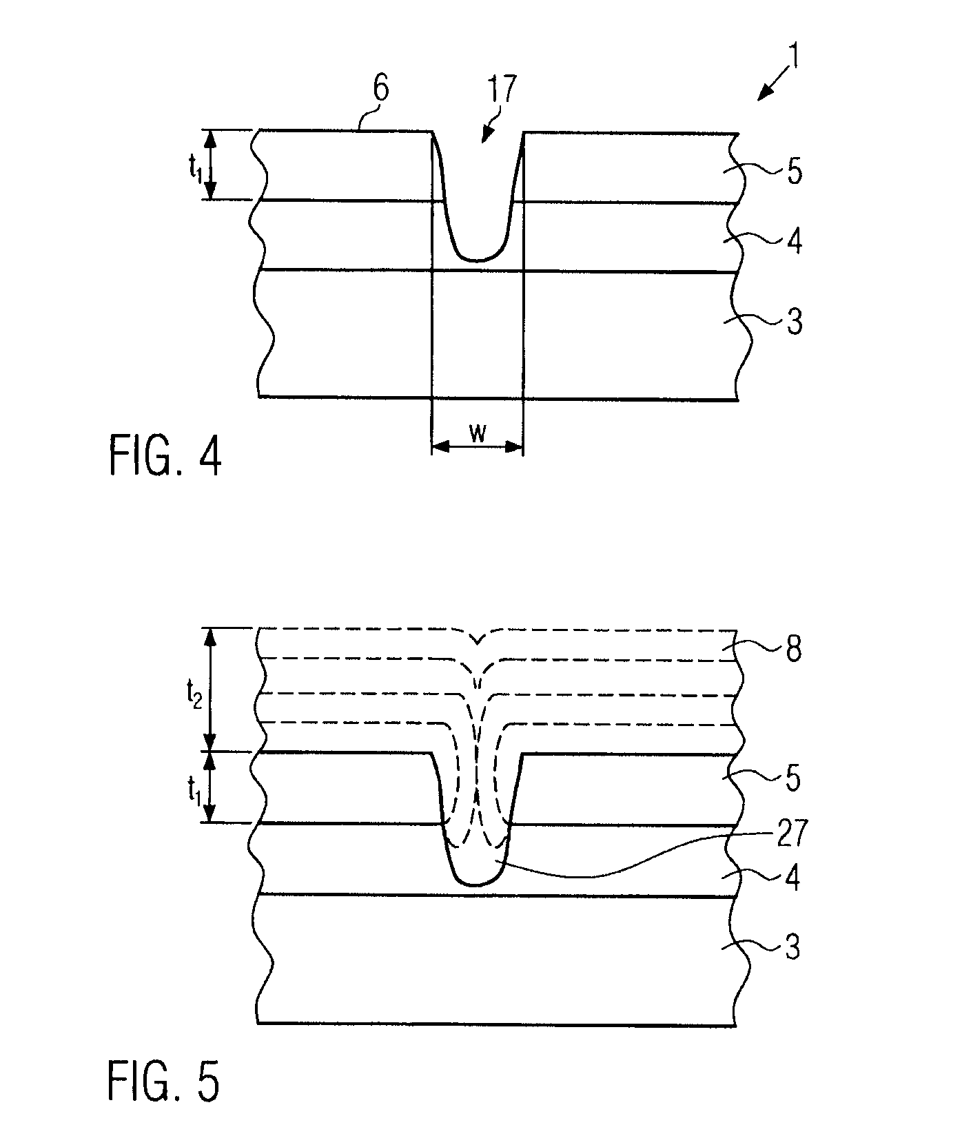
[0026]FIG. 1 schematically shows a SOI substrate 1 containing at least one defect such as a HF-defect or the shown oxide precipitate 2. The SOI substrate 1 is only shown exemplarily to demonstrate the principle of the present invention, wherein the present invention can also be used to improve the surface quality of another semiconductor substrate like a silicon wafer or any other substrate having on top at least partially silicon. In particular, it is not necessary to provide a substrate with an oxide layer, as shown in FIG. 1, to apply the inventive idea of repairing this substrate.

[0027]The inventive method is also applicable to other materials such as silicon alloys, for example SiGe structures.

[0028]The SOI substrate of FIG. 1 comprises a silicon substrate 3, on which a buried oxide 4 is formed, and has on top a silicon layer 5 having a certain thickness t1 and comprising the at least one defect such as the shown oxide precipitate 2 situated at a surface 6 of the silicon layer ...


PUM


Abstract

The invention relates to a method of improving a surface of a semiconductor substrate which is at least partially made of silicon. Defects present in or on the semiconductor substrate can be really repaired to provide a semiconductor substrate with a high surface quality. This is achieved by a selective epitaxial deposition in the at least one hole in the surface of the semiconductor substrate. Generally, the deposition step is preceded by an etching step which removes the defects and leaves behind at least one hole that can be plugged or filled with the selective epitaxial deposition of silicon to repair the substrate.

Description

BACKGROUND ART[0001]The invention relates to a method of improving a surface of a semiconductor substrate, wherein the surface at least partially includes silicon.[0002]In semiconductor device production, it is more and more important to provide semiconductor substrates of a very high quality. Defects of semiconductor substrates can be of very different origin and may occur in the bulk material of wafers or layers or on the surface of a structure. Deficient wafers, such as wafers or layers with holes or scratches on their surface or with oxide precipitates or so-called “HF-defects”, which are present in or on a wafer and will be apparent by an HF-etch step, are mostly not suitable for further use.[0003]To improve the surface characteristic of a defective wafer, a wafer treatment of a wafer surface such as an etching step or a chemical mechanical polishing (“CMP”) step can be used to remove or to reduce the number or the size of defects at or near the wafer surface. Typical etchants ...

Claims


Application Information

Patent Timeline
IPC IPC(8): H01L21/322
CPCH01L21/02636H01L21/302H01L21/304
Inventor LIN, WEN
Owner SOITEC
Why Eureka
Try Eureka