Cleaning processes in the formation of integrated circuit interconnect structures

a technology of interconnect structure and cleaning process, which is applied in the manufacture of basic electric elements, electric devices, semiconductor/solid-state devices, etc., can solve the problems of limiting the speed of the integrated circuit, the gap between metal lines, and the increase of rc delay, so as to reduce the enlargement of the trench, the effect of small shift in the low-k dielectric properties

Inactive Publication Date: 2008-05-29
TAIWAN SEMICON MFG CO LTD
View PDF5 Cites 112 Cited by
  • Summary
  • Abstract
  • Description
  • Claims
  • Application Information

AI Technical Summary

Benefits of technology

[0010]The advantageous features of the present invention include small...

Problems solved by technology

A significant problem in the formation of interconnect structures is the parasitic capacitances between metal lines.
Parasitic capacitances cause an increase in RC delay.
In some high-speed circuits, interconnect capacitances can be the limiting factor in the speed of the integrated circuit.
However, it has been found that low-k materials are often subject to damage during the formation of inte...

Method used


Image

  • Cleaning processes in the formation of integrated circuit interconnect structures
  • Cleaning processes in the formation of integrated circuit interconnect structures
  • Cleaning processes in the formation of integrated circuit interconnect structures

Examples


Embodiment Construction

[0016]The making and using of the presently preferred embodiments are discussed in detail below. It should be appreciated, however, that the present invention provides many applicable inventive concepts that can be embodied in a wide variety of specific contexts. The specific embodiments discussed are merely illustrative of specific ways to make and use the invention, and do not limit the scope of the invention.

[0017]A novel method for forming an interconnect structure is provided. The intermediate stages for manufacturing the preferred embodiment of the present invention are illustrated. Throughout the various views and illustrative embodiments of the present invention, like reference numbers are used to designate like elements.

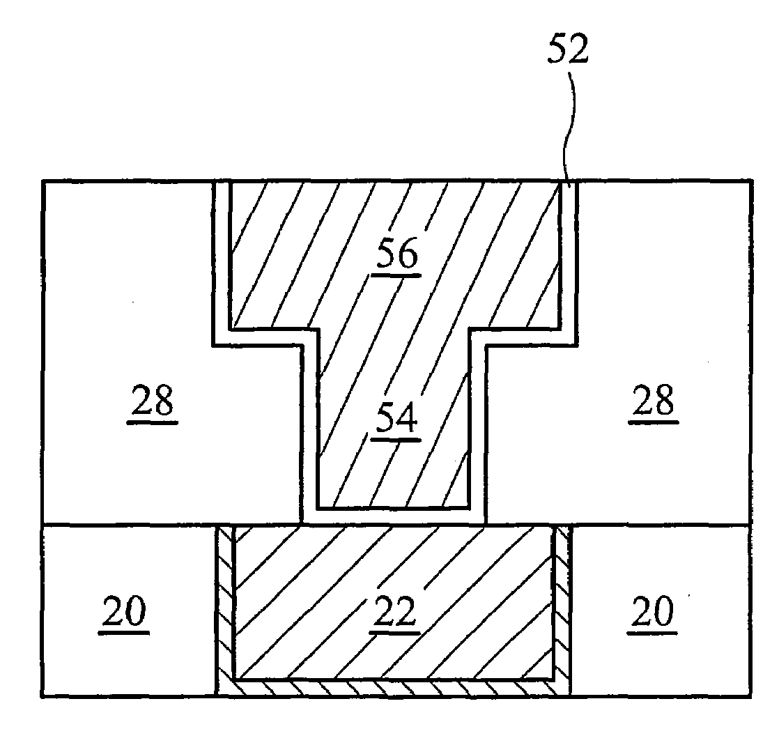
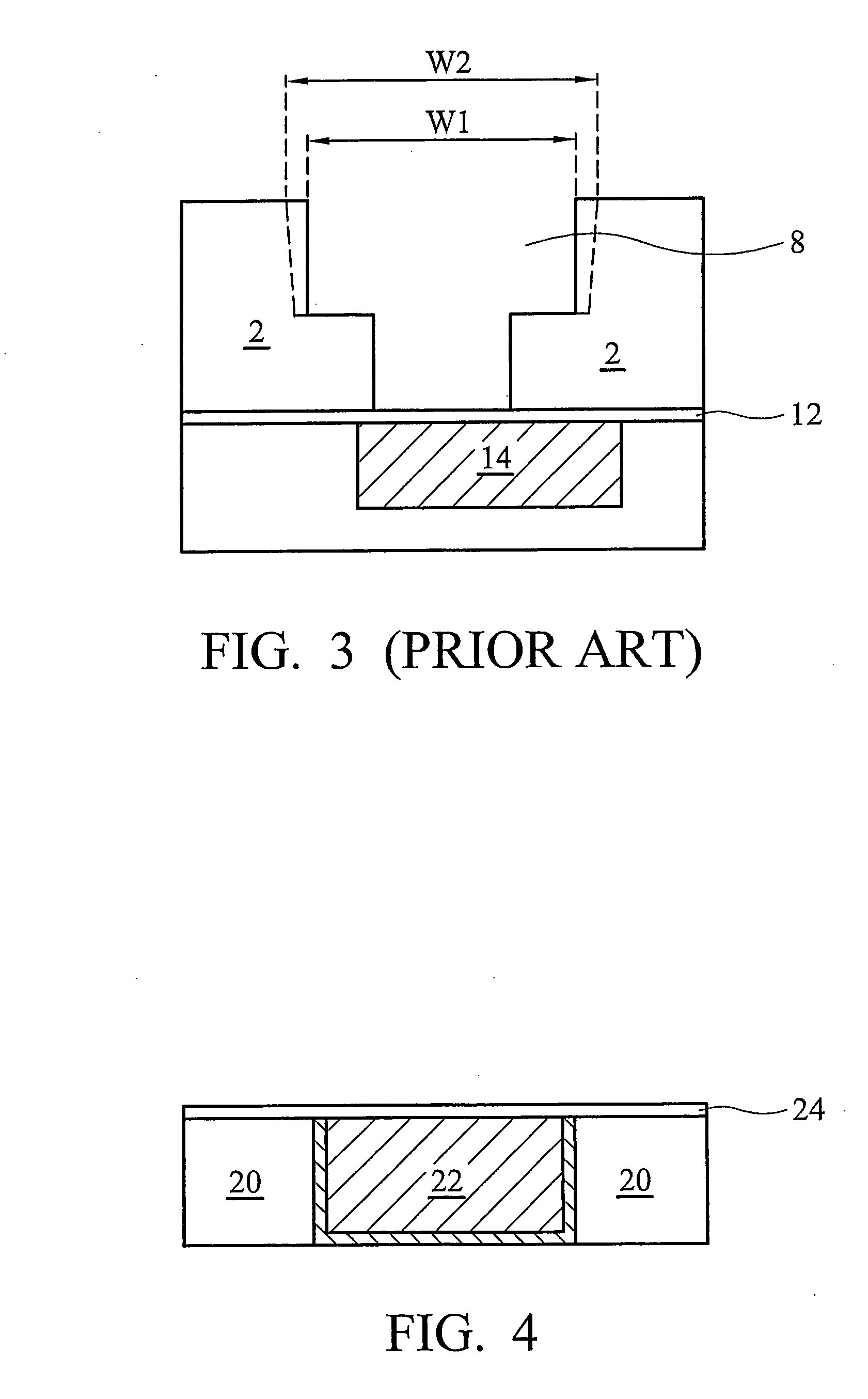
[0018]FIG. 4 illustrates a starting structure having a conductive line 22 formed in a dielectric layer 20. Conductive line 22 and dielectric layer 20 are over a semiconductor substrate (not shown), which is preferably a silicon substrate having semiconductor...


PUM


Abstract

A method for fabricating an integrated circuit includes providing a substrate, forming a low-k dielectric layer over the substrate, etching the low-k dielectric layer to form an opening in the low-k dielectric layer wherein an underlying metal is exposed through the opening, performing a remote plasma treatment to the substrate wherein a plasma used for the remote plasma treatment is generated from a plasma generator separated from a chamber in which the substrate is located, forming a diffusion barrier layer in the opening, and filling the opening with a conductive material. The method preferably includes an in-situ plasma treatment in a same chamber as the step of etching the low-k dielectric layer.

Description

TECHNICAL FIELD[0001]This invention is related generally to integrated circuits, and more particularly to the fabrication processes of interconnect structures in integrated circuits.BACKGROUND[0002]Conductive lines or interconnect structures are used to connect devices in integrated circuits and to connect to external pads. A significant problem in the formation of interconnect structures is the parasitic capacitances between metal lines. Parasitic capacitances cause an increase in RC delay. In some high-speed circuits, interconnect capacitances can be the limiting factor in the speed of the integrated circuit. Thus it is desirable to reduce the interconnect capacitances. Accordingly, low dielectric constant (low-k) materials have been increasingly used. However, it has been found that low-k materials are often subject to damage during the formation of interconnect structures.[0003]FIGS. 1 and 2 illustrate cross-sectional views in the manufacture of a typical interconnect structure....

Claims


Application Information

Patent Timeline
IPC IPC(8): H01L21/4763
CPCH01L21/02063H01L21/76814H01L21/76807
Inventor HUANG, CHENG-LINHSIEH, CHING-HUASHUE, SHAU-LIN
Owner TAIWAN SEMICON MFG CO LTD
Why Eureka
Try Eureka