Method, system and computer program for automated hardware design debugging

a hardware design and debugging technology, applied in the field of hardware debugging, can solve the problems of consuming over 30% of the design effort, tedious, time-consuming and costly manual process, and simulation engines that cannot be used to prove the correctness of a design. , to achieve the effect of large designs

Inactive Publication Date: 2008-05-29
VENERIS ANDREAS +3
View PDF20 Cites 30 Cited by
  • Summary
  • Abstract
  • Description
  • Claims
  • Application Information

AI Technical Summary

Benefits of technology

[0018]According to one embodiment, the diagnosis problem is formulated as a Quantified Boolean Formula (QBF), allowing large designs to be handled in a memory efficient manner. The QBF approach can accom

Problems solved by technology

Design debugging is considered a major bottleneck in the overall hardware design cycle which consumes over 30% of the design effort.
This is a tedious, time consuming and costly manual process.
In practice, simulation engines can rarely be used to prove the correctness of a design.Formal verification tools.
However, the approach is not automated, requiring the constant input of a user.
These are example of diagnosis meth

Method used


Image

  • Method, system and computer program for automated hardware design debugging
  • Method, system and computer program for automated hardware design debugging
  • Method, system and computer program for automated hardware design debugging

Examples


Embodiment Construction

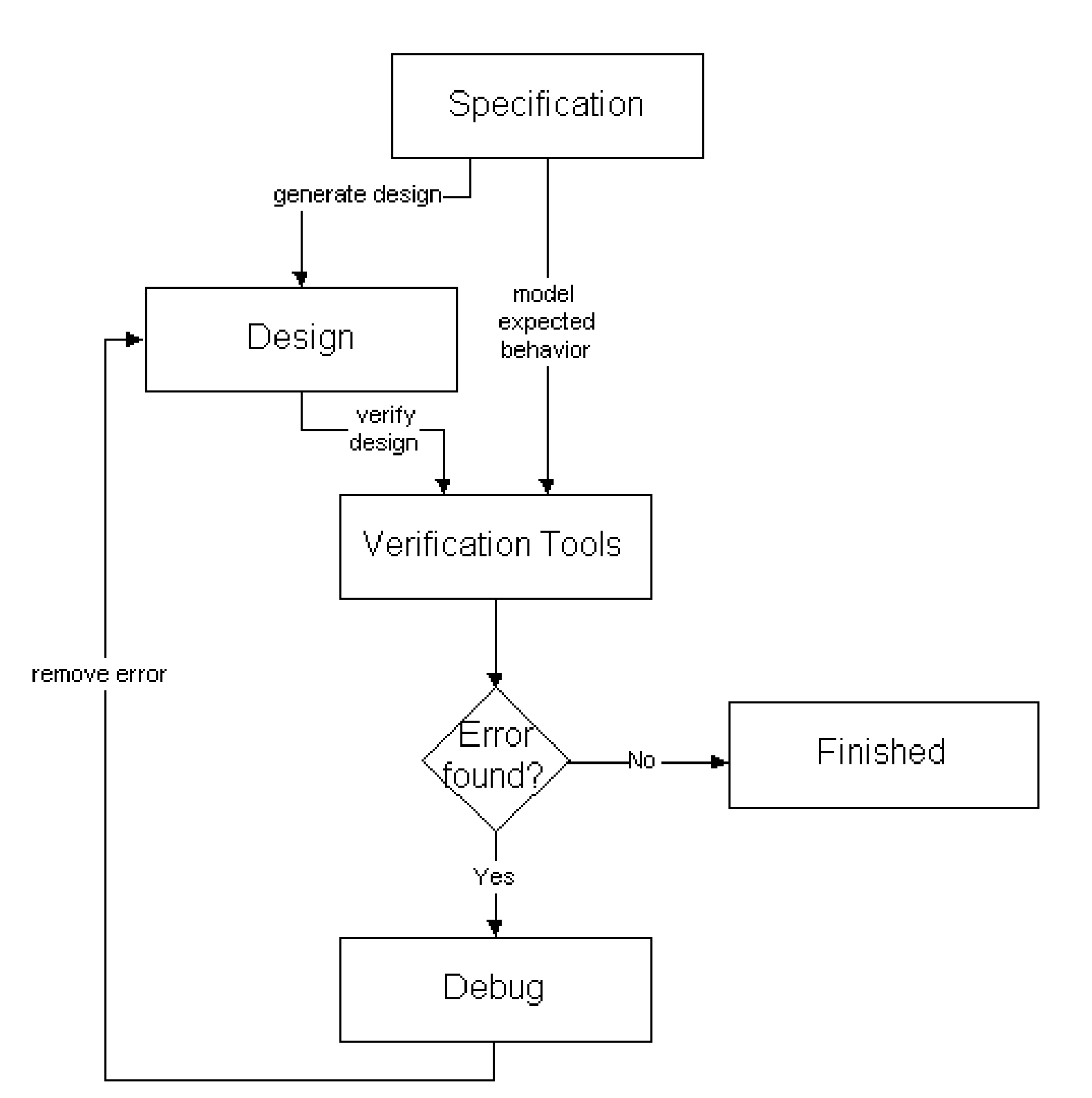
[0034]The present invention provides an automated hardware design debugging approach implemented as a method, system and computer program.

[0035]Generally speaking, the overall process of finding the source of errors in a design at the HDL level is referred to as “debugging” and the process of locating the error sources at the gatelevel and logic level is referred to as “diagnosis”.

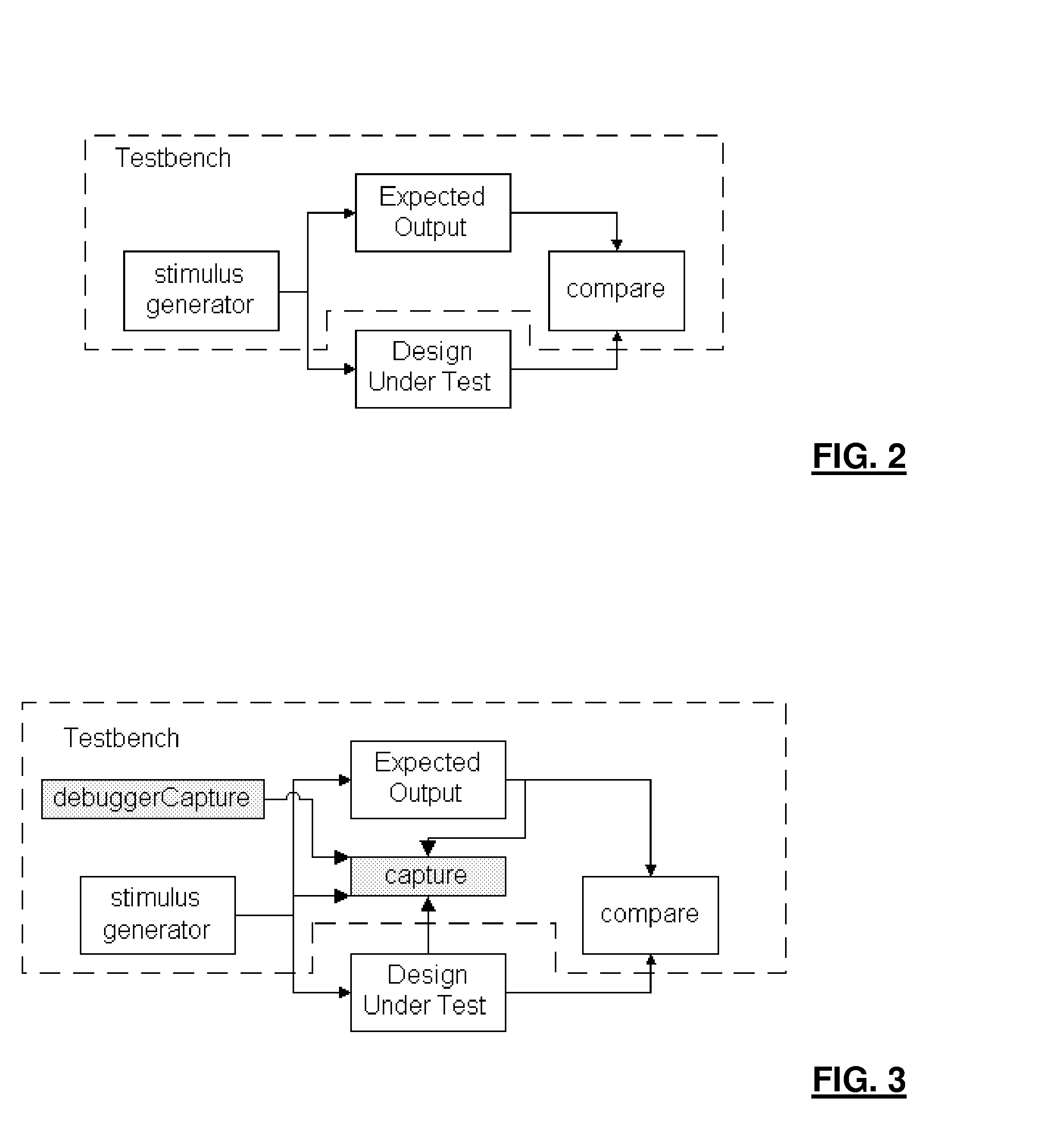
[0036]The present invention first interacts with the verification environment and retrieves information required to perform diagnosis. This is referred to as the “Capture Information”. Once the Capture Information is available, a diagnosis problem is constructed which can be solved using existing techniques or new techniques, as described herein. Finally, a logic-HDL map is used to translate solutions of the diagnosis problem to the HDL-level where the user can identify the error sources.

[0037]This automated debugging approach is different from the existing manual debugging processes described above becaus...


PUM


Abstract

The present invention provides a method, system and computer program for automated debugging for pre-fabricated digital synchronous hardware designs implemented in Hardware Description Language (HDL). Required information is captured by interacting with the verification environment after verification fails. This capture information is used to build a diagnosis problem where the solution is a set of logic level error sources. Using the HDL information, the error at the logic level is translated to gates, modules, statements, and signals in the HDL description. The diagnosis problem can be solved efficiently formulating a Quantified Boolean Formula (QBF) problem and also by using the hierarchical and modular nature of the HDL design during diagnosis.

Description

FIELD OF THE INVENTION[0001]The present invention relates to the field of hardware debugging. The present invention more particularly relates to debugging hardware designs implemented in Hardware Description Language (HDL).BACKGROUND OF THE INVENTION[0002]Hardware design debugging is the process of finding or locating errors in designs after verification methodologies and techniques determine the presence of such errors. Design debugging is considered a major bottleneck in the overall hardware design cycle which consumes over 30% of the design effort. Today, design debugging is performed almost exclusively manually by hardware designers and verification engineers using graphical navigation tools. This is a tedious, time consuming and costly manual process.[0003]A typical hardware design cycle starts with a specification document which describes the functionality, timing and general constraints of the design. The specification is used to both create the design, typically implemented ...

Claims


Application Information

Patent Timeline
IPC IPC(8): G06F17/50
CPCG06F17/504G06F11/3608G06F30/3323
Inventor VENERIS, ANDREASSAFARPOUR, SEANFAHIM ALI, MOAYAD YEHIAMANGASSARIAN, HRATCH
Owner VENERIS ANDREAS
Why Eureka
Try Eureka