Semiconductor Device and Method of Manufacturing the Same

a technology of semiconductors and semiconductors, applied in the direction of semiconductor devices, electrical devices, transistors, etc., can solve the problems of large number of processes and components, difficulty in reducing costs,

Active Publication Date: 2008-06-12
SEMICON COMPONENTS IND LLC
View PDF6 Cites 36 Cited by
  • Summary
  • Abstract
  • Description
  • Claims
  • Application Information

AI Technical Summary

Problems solved by technology

This causes a large number of processes and co

Method used


Image

  • Semiconductor Device and Method of Manufacturing the Same
  • Semiconductor Device and Method of Manufacturing the Same
  • Semiconductor Device and Method of Manufacturing the Same

Examples


Embodiment Construction

[0028]A semiconductor device of an embodiment of this invention and a method of manufacturing that device will be described in detail referring to figures.

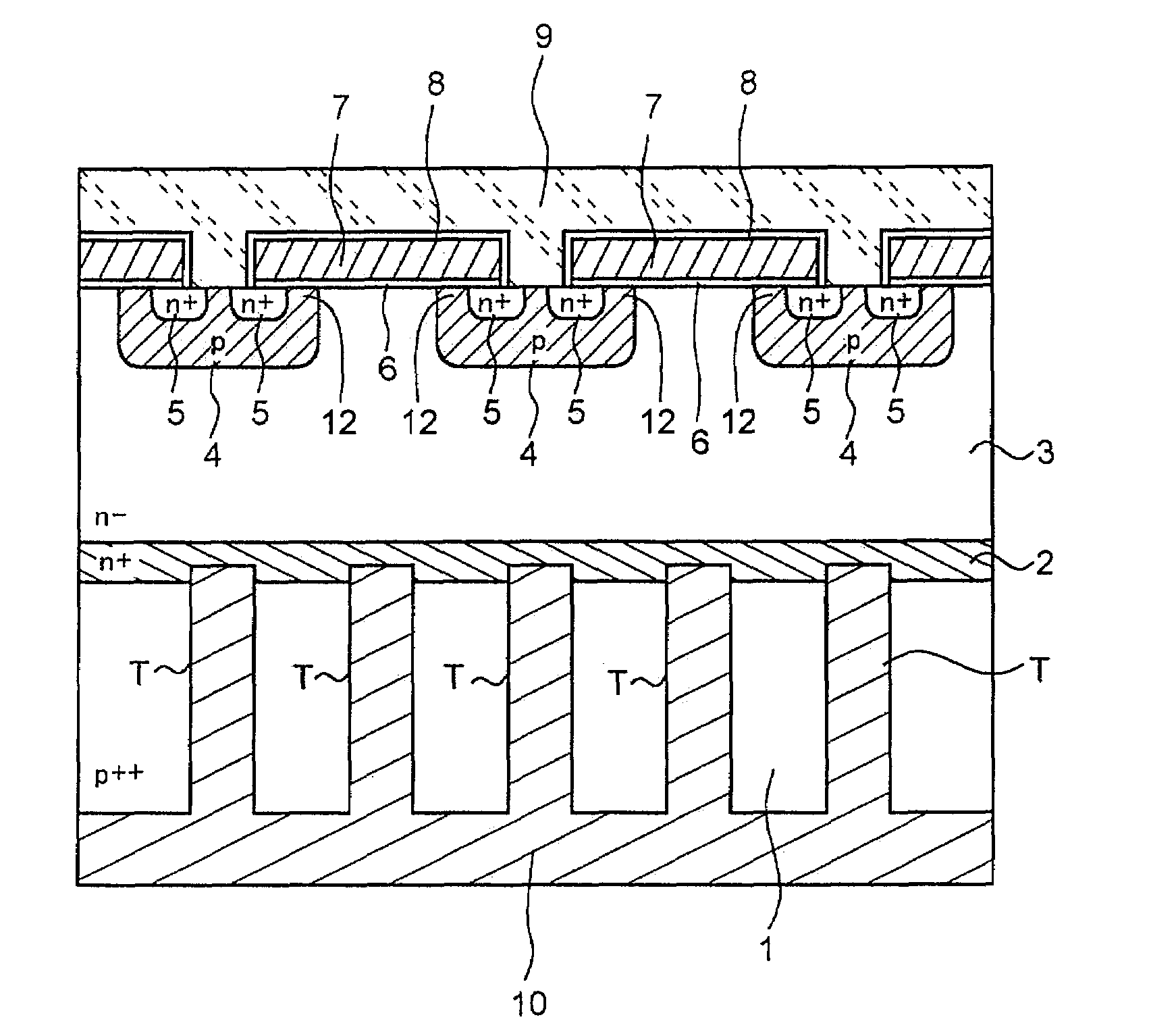
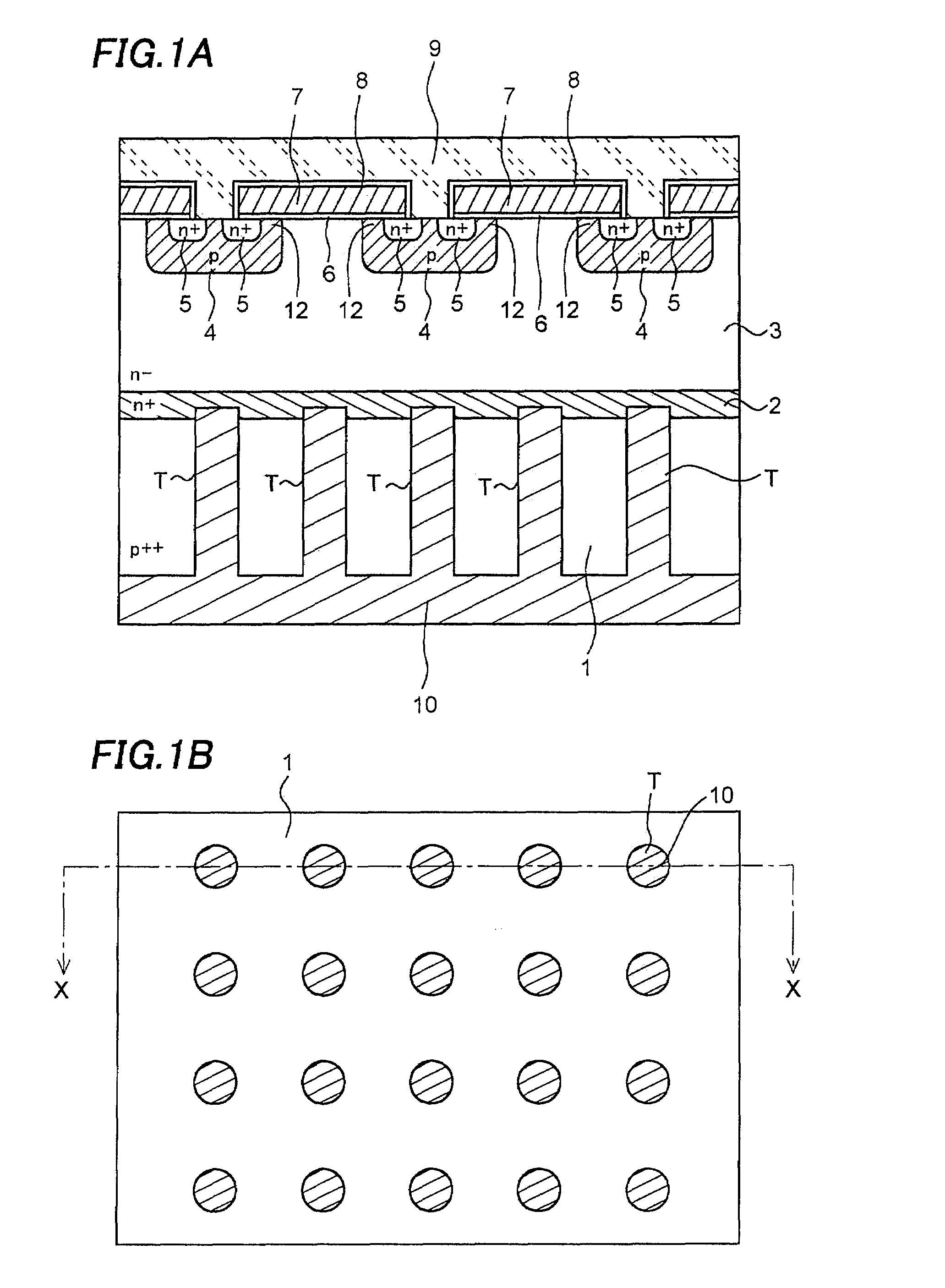
[0029]First, a structure of the semiconductor device of the embodiment will be described. FIG. 1B shows a plane view of the semiconductor device of the embodiment. FIG. 1A shows a cross-sectional view of the semiconductor device, more specifically, a cross-sectional view of a punch-through type IGBT at line X-X in FIG. 1B

[0030]This cross-sectional view shows one unit cell only, but a number of unit cells are connected in parallel actually.

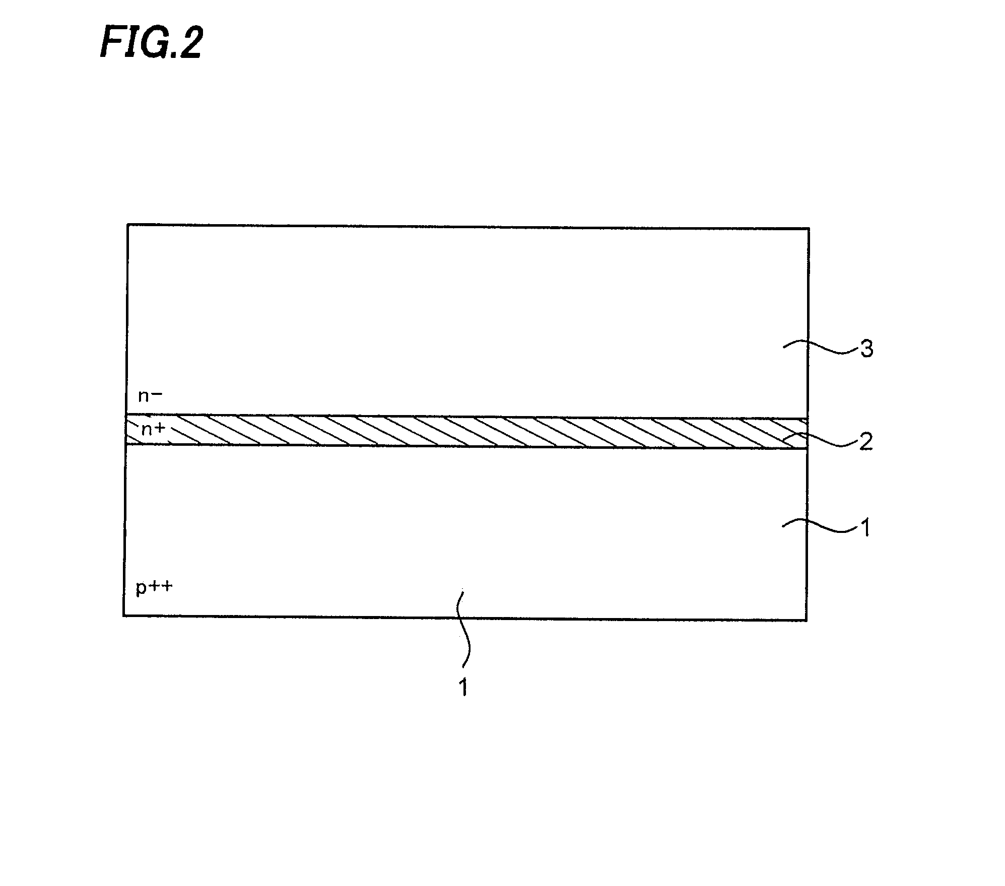
[0031]An n+-type buffer layer 2 and an n−-type drift layer 3 are formed on the front surface side of a p++-type semiconductor substrate (a collector layer 1) by epitaxial growth. The collector layer 1 and the drift layer 3 are about 150 μm and 50 μm in thickness, respectively.

[0032]It is noted that conductivity types such as p+, p and p− belong in a general conductivity type, and conductivity typ...


PUM


Abstract

A punch-through type IGBT generally has a thick p++-type collector layer. Therefore, the FWD need be externally attached to the IGBT when the IGBT is used as a switching element in an inverter circuit for driving a motor load, and thus the number of processes and components increases. In the invention, trenches are formed penetrating through a collector layer and reaching a buffer layer. A collector electrode is formed in the trenches, too. With this structure, a current path is formed between an emitter electrode and the collector electrode without through the collector layer and functions as the FWD.

Description

CROSS-REFERENCE OF THE INVENTION[0001]This application claims priority from Japanese Patent Application No. 2006-298524, the content of which is incorporated herein by reference in its entirety.BACKGROUND OF THE INVENTION[0002]1. Field of the Invention[0003]The invention relates to a semiconductor device and a method of manufacturing the same, particularly, a semiconductor device having an insulated gate bipolar transistor (IGBT) and a method of manufacturing the same.[0004]2. Description of the Related Art[0005]An insulated gate bipolar transistor is called IGBT, in which a fundamental cell combines the bipolar transistor and the MOS transistor, forming a semiconductor device having both low on-voltage characteristics of the former and voltage drive characteristics of the latter.[0006]FIG. 10 shows a conventional semiconductor device, more specifically, a cross-sectional view of a punch-through type IGBT. This cross-sectional view shows one unit cell only, but a number of unit cell...

Claims


Application Information

Patent Timeline
IPC IPC(8): H01L29/739H01L21/331
CPCH01L29/0657H01L29/0696H01L29/0834H01L29/7395H01L29/456H01L29/66333H01L29/41741H01L29/0821H01L29/41708
Inventor OKADA, KIKUOKAMEYAMA, KOJIRO
Owner SEMICON COMPONENTS IND LLC
Why Eureka
Try Eureka