Package structure for lead-free process

a lead-free, packaging technology, applied in the direction of manufacturing tools, solid-state devices, semiconductor/solid-state device details, etc., can solve the problems of reducing the reliability and lifetime of electronic products, affecting the reliability of electronic products, and cracking of the package structure, so as to improve the reliability, the lifetime and yield of the package structure can be increased, and the thermal durability can be improved.

Inactive Publication Date: 2008-06-19
DELTA ELECTRONICS INC
View PDF2 Cites 0 Cited by
  • Summary
  • Abstract
  • Description
  • Claims
  • Application Information

AI Technical Summary

Benefits of technology

[0008]In view of the foregoing, the invention is to provide a package structure suitable for the lead-free process, which can solve the crack problem of the package structure caused by the poor thermal durability in the lead-free process. Thus, the reliability, lifetime and yield of the package structure can be increased and the manufacturing cost can be decreased.
[0009]In addition, the invention is also to provide a package structure suitable for the lead-free process, which can minimize the size of the electronic products and occupy less space on the circuit board.
[0011]As mentioned above, the package structure of the invention includes a package portion having an extension protruding from the molding area, so that the pins of the electronic element can extend from the molding area and contact the extension of the first package portion. Compared with the prior art, the invention can buffer the thermal expansion effect during the lead-free process by the different sizes of the package portions, and the unchanged layout of the electronic element on the circuit board. Thus, the crack of the package structure can be prevented, and the package structure can have better thermal durability in the leadless process. Accordingly, the reliability, lifetime and yield of the package structure can be increased and the manufacturing cost can be decreased.

Problems solved by technology

However, the lead-free process is usually operated around 260° C. Therefore, if the thermal durability of the package portions 11 and 12 is poor, the package structure may crack and the electronic element may be damaged.
These problems will decrease the reliability and lifetime of the electronic products.

Method used


Image

  • Package structure for lead-free process
  • Package structure for lead-free process
  • Package structure for lead-free process

Examples


Embodiment Construction

[0018]The present invention will be apparent from the following detailed description, which proceeds with reference to the accompanying drawings, wherein the same references relate to the same elements.

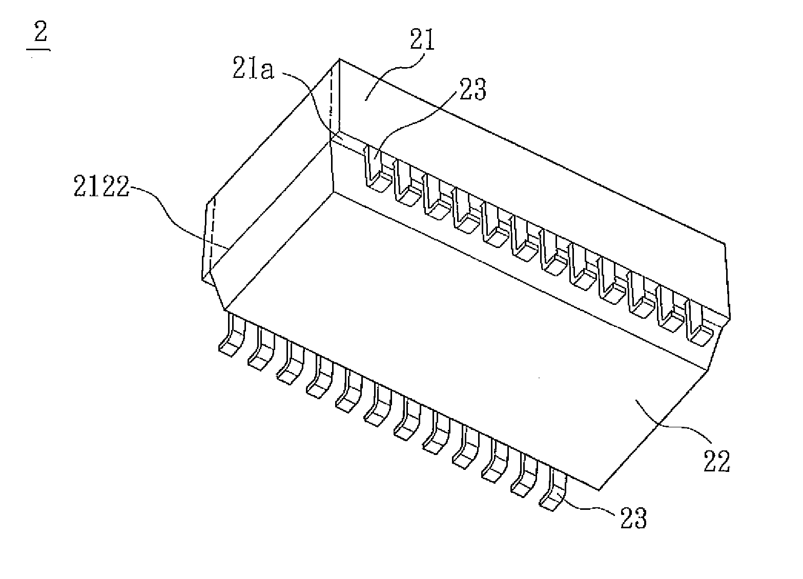
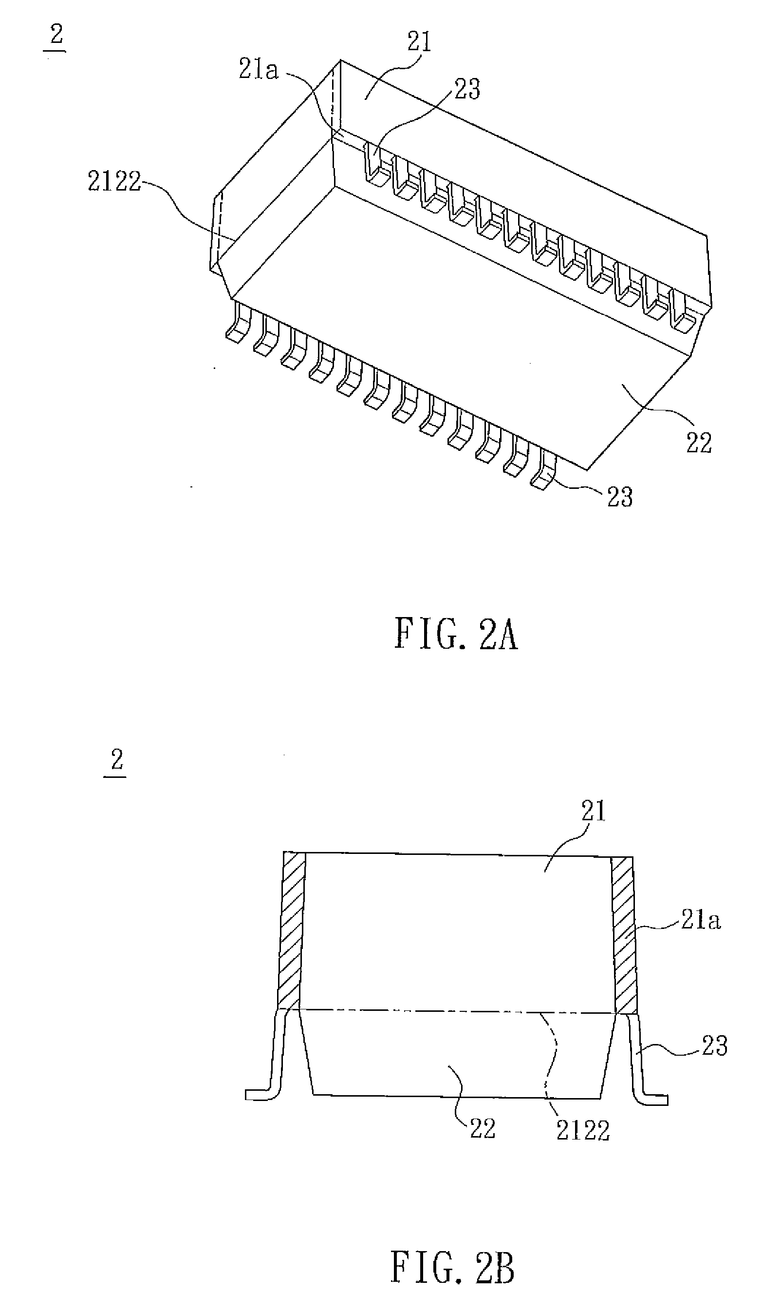
[0019]With reference to FIGS. 2A and 2B, a package structure 2 for a lead-free process according to an embodiment of the invention includes an electronic element (not shown), a first package portion 21 and a second package portion 22. The electronic element has a plurality of pins 23. In the embodiment, the package structure 2 is a surface mounted device (SMD). The first package portion 21 and second package portion 22 can be polygon and made of the same material such as a resin (e.g. epoxy). In addition, the first package portion 21 and second package portion 22 can be manufactured by press molding or injection molding, and they can be formed in a single process or separate processes. The first package portion 21 and second package portion 22 are connected to encapsulate the electron...


PUM

PropertyMeasurementUnit
package structureaaaaaaaaaa
temperatureaaaaaaaaaa
thermal durabilityaaaaaaaaaa

Abstract

A package structure for lead-flee process includes at least one electronic element, a first package portion and a second package portion. The electronic element has a plurality of pins. The second package portion and the first package portion are joined to encapsulate the electronic element and to form a molding area there between. The first package portion has an extension protruding from the molding area. The pins extend from the molding area and contact the extension of the first package portion.

Description

CROSS REFERENCE TO RELATED APPLICATIONS[0001]This Non-provisional application claims priority under 35 U.S.C. §119(a) on Patent Application No(s). 095147376 filed in Taiwan, Republic of China on Dec. 18, 2006, the entire contents of which are hereby incorporated by reference.BACKGROUND OF THE INVENTION[0002]1. Field of Invention[0003]The invention relates to a package structure and, in particular, to a package structure for a lead-free process.[0004]2. Related Art[0005]The environmental protection is one of the most considerations in the recent years. Regarding to this issue, many electronic products have been manufactured with lead-free materials and by lead-free manufacturing processes. In a lead-free process, such as a soldering process for mounting a surface mounted device (SMD) on a circuit board, the solder process provides a high temperature and it is easier to melt the SMD and the circuit board, so the thermal durability of the SMD and the circuit board must be enhanced. As ...

Claims


Application Information

Patent Timeline
Patent Type & Authority Applications(United States)
IPC IPC(8): B23K31/02
CPCH01L23/3107H01L2924/0002H01L2924/00
Inventor WANG, JUNLI, XIN-HUA
Owner DELTA ELECTRONICS INC
Why Eureka
Try Eureka