Transparent conductive multi-layer structure, process for its manufacture and device making use of transparent conductive multi-layer structure

a technology of transparent conductive and multi-layer structure, which is applied in the direction of conductive layers on insulating supports, sustainable manufacturing/processing, paper/cardboard containers, etc., can solve the problems of low electricity generation efficiency, low conductivity, and large light transmittance of electrodes, and achieve low film surface resistivity, good conductivity, and poor heat resistance

Inactive Publication Date: 2008-11-06
SUMITOMO METAL MINING CO LTD
View PDF4 Cites 12 Cited by
  • Summary
  • Abstract
  • Description
  • Claims
  • Application Information

AI Technical Summary

Benefits of technology

[0014]The present invention has been made taking account of the circumstances in such conventional cases. Accordingly, an object of the present invention is to proved a transparent conductive multi-layer structure which can be formed by a low-temperature film formable coating method, and has a transparent conductive layer and an auxiliary electrode layer, which transparent conductive layer has a smooth surface and also a very low film surface resistivity; a process for manufacturing the transparent conductive multi-layer structure; and low-cost devices in which the transparent conductive multi-layer structure is used.
[0021]Thus, according to the transparent conductive multi-layer structure of the present invention, a transfer process is applied, where the transparent conductive layer and the auxiliary electrode layer which have been formed on the smooth base material by coating are joined to the transparent substrate through the adhesive layer, and the smooth base material is removable by peeling. Hence, the peeled-off surface (base material peeled-off surface) of the transparent conductive layer from which the smooth base material has been peeled off can sufficiently be smooth, and also the transparent conductive layer shows a very good conductivity because it has the auxiliary electrode layer. Accordingly, devices can be formed on the smooth surface (peeled-off surface) without any restrictions at all. Furthermore, the transparent conductive layer and the auxiliary electrode layer are formed by a low-temperature film formable method, e.g., by coating, and hence this enables use of transparent substrates having a poor heat resistance, such as plastic films.
[0022]The device in which the transparent conductive multi-layer structure of the present invention is used, as exemplified by the dye-sensitized solar cell and the organic EL device, a very low film surface resistivity is achievable in virtue of the combination of the transparent conductive layer and the auxiliary electrode layer. Also, the auxiliary electrode layer is positioned between the transparent conductive layer and the transparent substrate, and the surface of the transparent conductive layer on its side where devices are to be formed can be very smooth to have no unevenness or protrusions present thereon. Hence, any electrical short circuit by no means occur between device electrodes. Thus, a dye-sensitized solar cell and an organic EL device can be provided which have transparent electrode layers having a very low film surface resistivity, can enjoy a low cost and can be of large area. Especially when used in the dye-sensitized solar cell, the auxiliary electrode can be prevented from corroding, because the auxiliary electrode is positioned on the side opposite to the electrolyte, interposing the transparent conductive layer.

Problems solved by technology

However, if the dye-sensitized solar cell is one having a size of 10 cm square or more than that, the electric current is consumed as Joule heat at the transparent electrode portion, and hence this lowers electricity generation efficiency extremely.
In such a case, however, because of the large layer thickness, the transparent electrode has a vastly low light transmittance and also a low electricity generation efficiency, and hence it is not practical to do so.
In the case of the dye-sensitized solar cell, however, the iodide-based electrolyte used as the electrolyte is very highly corrosive, and hence, not to speak of silver and copper, even gold is not usable.
However, such an auxiliary electrode layer must be formed in a layer thickness of several microns to tens of microns (μm) in order for that layer to achieve the intended function, and hence it follows that unevenness (hills and dales) of several microns to tens of microns (μm) in extent comes about on the side where devices are to be formed on the transparent conductive layer.
This brings about great restrictions on the formation of devices (e.g., devices must be formed only in areas where any pattern-shaped auxiliary electrode layer is not formed).
Hence, there has also been a limit to how the transparent electrode is made to have a low film surface resistivity.
Hence, it has been difficult to achieve a sufficient protective effect without making devices have poor characteristics.
In this case as well, however, like the case of the dye-sensitized solar cell, there has been a problem that the unevenness due to the formation of such an auxiliary electrode layer brings about great restrictions in regard to the fabrication of devices.
Moreover, conventional transparent conductive layers used in the dye-sensitized solar cell and organic EL device are formed by film forming processes such as sputtering and CVD, which require large-size and expensive systems.
Hence, there have been problems that a very high cost results and besides it is difficult to form transparent conductive layers on transparent substrates having a poor heat resistance, such as plastic films.
However, the transparent conductive layer thus obtained has so high a film surface resistivity that it can not be said to be practical for its use in the devices such as the dye-sensitized solar cell.
However, the transparent conductive layer obtained has a film surface resistivity of about hundreds of Ω / square, which is still insufficient.

Method used


Image

  • Transparent conductive multi-layer structure, process for its manufacture and device making use of transparent conductive multi-layer structure
  • Transparent conductive multi-layer structure, process for its manufacture and device making use of transparent conductive multi-layer structure
  • Transparent conductive multi-layer structure, process for its manufacture and device making use of transparent conductive multi-layer structure

Examples


example 1

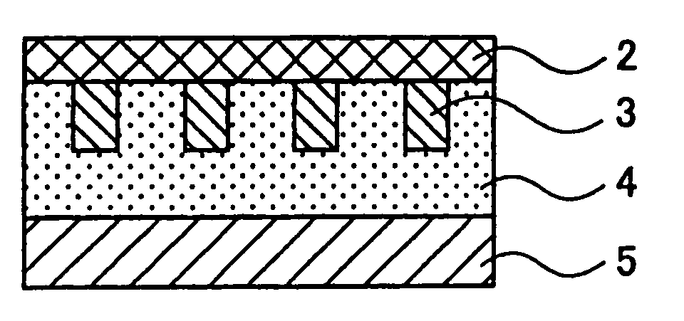
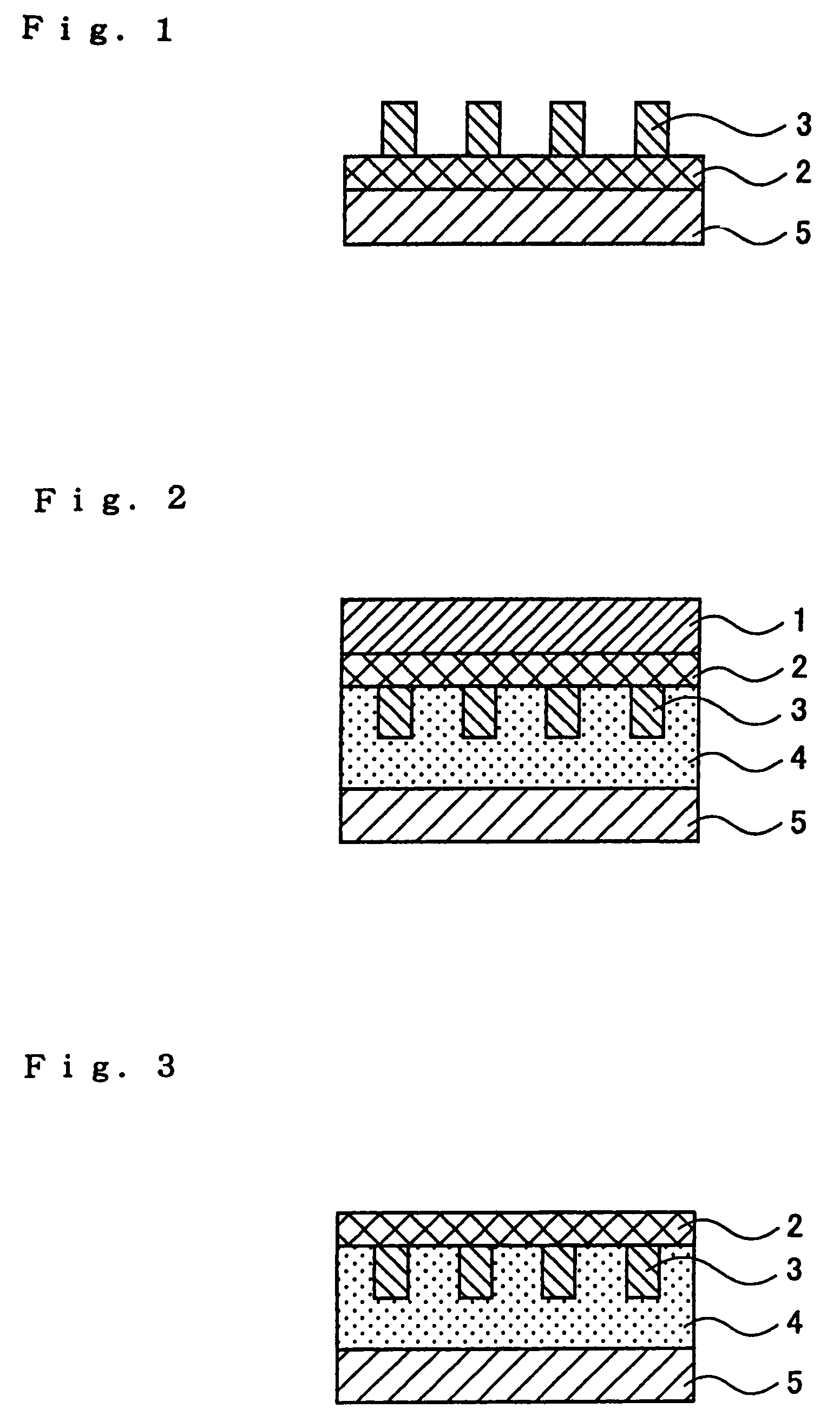
[0089]60 g of fine ITO particles of 0.03 μm in average particle diameter (trade name: SUFP-HX; available from Sumitomo Metal Mining Co., Ltd.) were mixed with 40 g of isophorone serving as a solvent, followed by dispersion treatment to obtain a transparent conductive layer forming coating fluid in which fine ITO particles of 110 nm in average dispersed-particle diameter stood dispersed. Meanwhile, as a smooth base material, PET film (trade name: LUMILAR; available from Toray Industries, Inc.; thickness: 100 μm) was used.

[0090]This smooth base material was coated with the transparent conductive layer forming coating fluid by wire bar coating (wire diameter: 0.3 mm), followed by heat treatment at 40° C. for 15 minutes and thereafter at 120° C. for 30 minutes to form on the smooth base material a transparent conductive layer (layer thickness: 3 μm) constituted of fine ITO particles. This transparent conductive layer had film properties of visible light transmittance: 80.3%; haze value:...

example 2

[0101]The same smooth base material as that in Example 1 was coated with the same transparent conductive layer forming coating fluid as that in Example 1 by wire bar coating (wire diameter: 0.15 mm), followed by drying at 40° C. for 15 minutes and thereafter at 120° C. for 10 minutes, and thereafter rolling (linear pressure: 147 N / mm=150 kgf / cm; nip width: 1 mm) by means of hard chromium electroplated steel rolls of 150 mm in diameter to form on the smooth base material a transparent conductive layer (layer thickness: 1.8 μm) constituted of densely filled, fine ITO particles. This transparent conductive layer had film properties of visible light transmittance: 90.9%; haze value: 2.1%; and film surface resistivity: 200 Ω / square.

[0102]The subsequent procedure in Example 1 was repeated except that the smooth base material was used on which the above transparent conductive layer was formed, to obtain a transparent conductive multi-layer structure.

[0103]The transparent conductive multi-l...

example 3

[0107]The procedure of Example 1 was repeated to form on the PET film as the smooth base material the transparent conductive layer constituted of fine ITO particles. On this transparent conductive layer, first, an auxiliary electrode layer forming paste in which fine carbon particles stood dispersed in a solvent together with a phenolic-resin binder (trade name of the paste: XC-223; available from Fujikura Kasei Co., Ltd.) was screen-printed (screen: 250 mesh) in a lattice (line width: 0.3 mm; line-to-line distance: 2.7 mm), followed by heat treatment at 90° C. for 5 minutes to form a first pattern-shaped auxiliary electrode layer (layer thickness: 15 μm) composed of fine carbon particles.

[0108]Thereafter, on the first pattern-shaped auxiliary electrode layer composed of fine carbon particles, an auxiliary electrode layer forming paste in which fine silver particles stood dispersed in a solvent together with a polyester resin binder (trade name of the paste: FA-401CA; available from...


PUM


Abstract

A transparent conductive multi-layer structure having a smooth base material 1, a transparent conductive layer 2 formed on the smooth base material 1 by coating, an auxiliary electrode layer 3 formed in a pattern on the transparent conductive layer 2, and a transparent substrate 5 joined to the transparent conductive layer 2 and auxiliary electrode layer 3 through an adhesive layer 4. On a smooth peeled-off surface of the transparent conductive layer 2 from which the smooth base material 1 has been peeled off, various devices are formed to set up devices such as a dye-sensitized solar cell and an organic electroluminescent device.

Description

CROSS PREFERENCE TO RELATED APPLICATION[0001]This application is a Divisional Application of prior application Ser. No. 10 / 576,881 filed on Apr. 21, 2006, which is a 371 national stage application of PCT / JP04 / 16054, filed on Oct. 22, 2004, which is hereby incorporated by reference.TECHNICAL FIELD[0002]This invention relates to a transparent conductive multi-layer structure usable in transparent electrode portions of devices such as dye-sensitized solar cells and organic electroluminescent devices, a process for its manufacture, and devices making use of the transparent conductive multi-layer structure.BACKGROUND ART[0003]In recent years, a dye-sensitized solar cell is proposed by Graetzel et al. (see National Publication No. H05-504023). This dye-sensitized solar cell can be fabricated by a simple process and may be constituted of inexpensive materials. Accordingly, there is a high possibility that it can be obtained at a lower cost than conventional silicon type solar cells, and st...

Claims


Application Information

Patent Timeline
Patent Type & Authority Applications(United States)
IPC IPC(8): B32B38/14B32B7/02H01B5/14H01B13/00H01G9/20H01L31/04H01L51/52H01M14/00H05B33/14H05B33/28
CPCH01G9/2022H01L51/003H01L51/5206H01L51/5237Y10T428/24942H01M14/005Y02E10/542Y10T156/10H01L2227/326Y02P70/50H10K71/80H10K50/814H10K50/8426H10K59/1201H10K50/844H10K50/846
Inventor YUKINOBU, MASAYA
Owner SUMITOMO METAL MINING CO LTD
Why Eureka
Try Eureka