Method for fabricating a power semiconductor device having a voltage sustaining layer with a terraced trench facilitating formation of floating islands
What is Al technical title?
Al technical title is built by PatSnap Al team. It summarizes the technical point description of the patent document.
a technology of power semiconductor and terraced trench, which is applied in the direction of semiconductor devices, basic electric elements, electrical equipment, etc., can solve the problems of high cost of epitaxial deposition steps, rapid increase in resistance of devices, and high cost of devices
Inactive Publication Date: 2008-06-19
VISHAY GENERAL SEMICONDUCTOR LLC
View PDF31 Cites 12 Cited by
Summary
Abstract
Description
Claims
Application Information
AI Technical Summary
This helps you quickly interpret patents by identifying the three key elements:
Problems solved by technology
Method used
Benefits of technology
Problems solved by technology
Unfortunately, as the curve shows, the on-resistance of the device increases rapidly as its breakdown voltage increases.
This rapid increase in resistance presents a problem when the MOSFET is to be operated at higher voltag
Method used
Image
Click on the blue label to locate the original text in one second.
Reading with bidirectional positioning of images and text.
Examples
Embodiment Construction
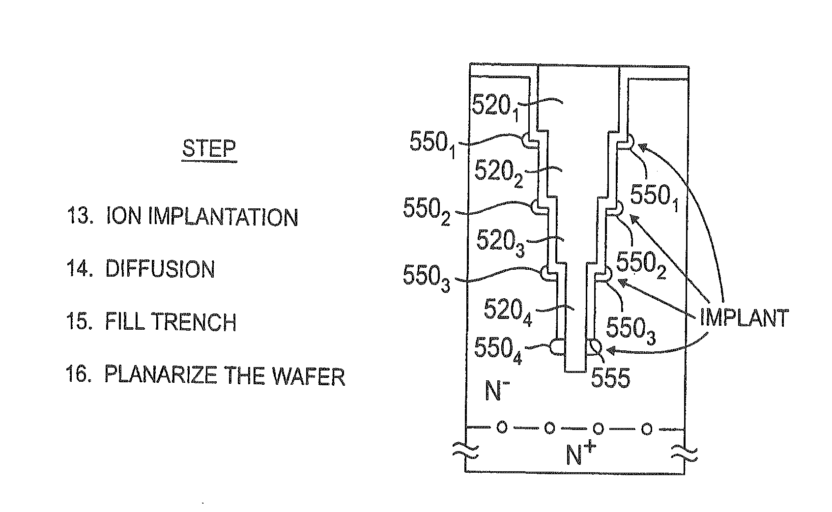
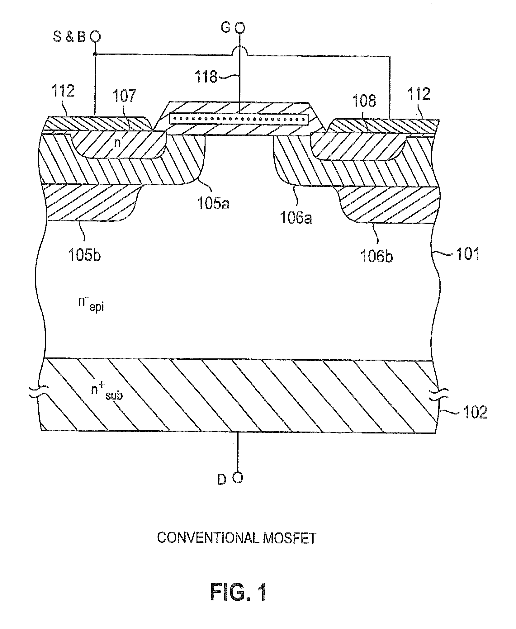
[0016]FIG. 4 shows a power semiconductor device having floating islands of the type disclosed in co-pending U.S. application Ser. No. [GS 158]. In this device the trenches are assumed to be circular and therefore the floating islands are depicted as donut-shaped. Of course, the trenches may have other shapes such squares, rectangles, hexagons, or the like, which in turn will determine the shape of the floating islands. An N-type epitaxial silicon layer 401 formed over an N+ silicon substrate 402 contains P-body regions 405, and N+ source regions 407 for two MOSFET cells in the device. As shown, P-body regions 405a may also include deep P-body regions 405b. A source-body electrode 412 extends across certain surface portions of epitaxial layer 401 to contact the source and body regions. The N-type drain for both cells is formed by the portion of N-epitaxial layer 401 extending to the upper semiconductor surface. A drain electrode is provided at the bottom of N+ substrate 402. An insul...
PUM
Abstract
A method is provided for forming a power semiconductor device. The method begins by providing a substrate of a second conductivity type and then forming a voltage sustaining region on the substrate. The voltage sustaining region is formed by depositing an epitaxial layer of a first conductivity type on the substrate and forming at least one terraced trench in the epitaxial layer. The terraced trench has a plurality of portions that differ in width to define at least one annular ledge therebetween. A barrier material is deposited along the walls of the trench. A dopant of a second conductivity type is implanted through the barrier material lining the annular ledge and said trench bottom and into adjacent portions of the epitaxial layer. The dopant is diffused to form at least one annular doped region in the epitaxial layer and at least one other region located below the annular doped region. A filler material is deposited in the terraced trench to substantially fill the trench, thus completing the voltage sustaining region. At least one region of the second conductivity type is formed over the voltage sustaining region to define a junction therebetween.
Description
RELATED APPLICATIONS[0001]This application is a continuation in part of U.S. patent application Ser. No. 10 / 712,810, filed Nov. 13, 2003, entitled “Method for Fabricating a Power Semiconductor Device Having a Voltage Sustaining Layer with a Terraced Trench Facilitating Formation of Floating Islands”, now U.S. Pat. No. 7,304,347, which is a divisional of U.S. patent application Ser. No. 09 / 970,758, filed Oct. 4, 2001, entitled “Method for Fabricating a Power Semiconductor Device Having a Voltage Sustaining Layer with a Terraced Trench Facilitating Formation of Floating Islands”, now U.S. Pat. No. 6,649,477, which is related to U.S. patent application Ser. No. 09 / 970,972, filed Oct. 4, 2001, entitled “Method for Fabricating a Power Semiconductor Device Having a Floating Island Voltage Sustaining Layer”, now U.S. Pat. No. 6,465,304. Each of the above applications is incorporated herein by reference in its entirety.FIELD OF THE INVENTION[0002]The present invention relates generally to s...
Claims
Application Information
Patent Timeline
Application Date:The date an application was filed.
Publication Date:The date a patent or application was officially published.
First Publication Date:The earliest publication date of a patent with the same application number.
Issue Date:Publication date of the patent grant document.
PCT Entry Date:The Entry date of PCT National Phase.
Estimated Expiry Date:The statutory expiry date of a patent right according to the Patent Law, and it is the longest term of protection that the patent right can achieve without the termination of the patent right due to other reasons(Term extension factor has been taken into account ).
Invalid Date:Actual expiry date is based on effective date or publication date of legal transaction data of invalid patent.