Multi-chip module, manufacturing method thereof, mounting structure of multi-chip module, and manufacturing method of mounting structure

a manufacturing method and multi-chip technology, applied in the direction of printed circuits, semiconductor devices, semiconductor/solid-state device details, etc., can solve the problems of insufficient connection between multi-chip modules b>120/b> and another substrate, and differences in the height of solder bumps due to the warpage of multi-chip modules, etc., to achieve the effect of reducing the warpag

Inactive Publication Date: 2008-06-26
SHARP KK
View PDF56 Cites 19 Cited by
  • Summary
  • Abstract
  • Description
  • Claims
  • Application Information

AI Technical Summary

Benefits of technology

[0013]The present invention was done to solve the problem above, and the objective of the present invention is to provide a multi-chip module which can reduce its warpage, a manufacturing method thereof, a mounting structure of the multi-chip module, and a manufacturing method of the structure.
[0015]According to the arrangement above, assuming that a part of the multi-chip module above the central plane which horizontally cuts the multi-chip module is an upper structure whereas the remaining part of the multi-chip module below the central plane is a lower structure, the arrangements in the upper structure and the arrangements in the lower structure are substantially plane symmetrical with respect to the central plane which horizontally cuts the multi-chip module. The upper and lower structures therefore warp in opposite directions. In other words, the upper and lower structures cancel out the warping forces of each other. Consequently the multi-chip module can reduce its warpage.
[0016]Furthermore, because the warpage of the multi-chip module is reduced, the multi-chip module can be surely connected to another substrate. Moreover, even if a temperature change occurs in the use environment after the mounting, connection failure between the substrate and the multi-chip module is restrained because the warpage of the multi-chip module is small.
[0018]According to the arrangement above, principal parts of the upper structure above the central plane which horizontally cuts the multi-chip module and principal parts of the lower structure below the central plane are substantially identical. Therefore in terms of the elongation and contraction in one direction due to temperature changes, the upper and lower structures are identical with each other. In other words, since the difference in the degree of elongation and contraction between the upper and lower structures is small, an in-plane stress is restrained. As a result, the warpage of the multi-chip module is reduced.
[0019]Furthermore, because the warpage of the multi-chip module is reduced, the multi-chip module can be surely connected to another substrate. Moreover, even if a temperature change occurs in the use environment after the mounting, connection failure between the substrate and the multi-chip module is restrained because the warpage of the multi-chip module is small.

Problems solved by technology

This conventional multi-chip module is disadvantageous in that the multi-chip module warps, because of the reason below.
Because of this warpage, connection between the multi-chip module 120 and another substrate cannot be sufficiently established.
Furthermore, if solder bumps are also provided at the central part of the multi-chip module, differences among the heights of solder bumps due to the warpage of the multi-chip module are more severe.
Therefore, a multi-chip module having a rectangular shape cannot be attached to a substrate even if the warpage of the module is slight.
In addition to this, as the size of a multi-chip module increases, attaching the multi-chip module to a substrate becomes more difficult.
Since these warps are intricately combined in the multi-chip module, the multi-chip module rarely warps evenly, i.e. typically warps unevenly.
As a result, it is very difficult to attach the multi-chip module to a substrate.
In addition to the above, considering all electronic components other than semiconductor chips, which are mounted on the multi-chip module, it is extremely difficult to make the sizes of these electronic components be even.
In particular, the uneven warpage of the multi-chip module is further significant when electronic components having different heights are provided therein.
Furthermore, the conventional multi-chip module does not take account of the relationship between the coefficient of linear expansion of the multi-chip module and the coefficient of linear expansion of the substrate to which the multi-chip module is attached.

Method used


Image

  • Multi-chip module, manufacturing method thereof, mounting structure of multi-chip module, and manufacturing method of mounting structure
  • Multi-chip module, manufacturing method thereof, mounting structure of multi-chip module, and manufacturing method of mounting structure
  • Multi-chip module, manufacturing method thereof, mounting structure of multi-chip module, and manufacturing method of mounting structure

Examples


embodiment 1

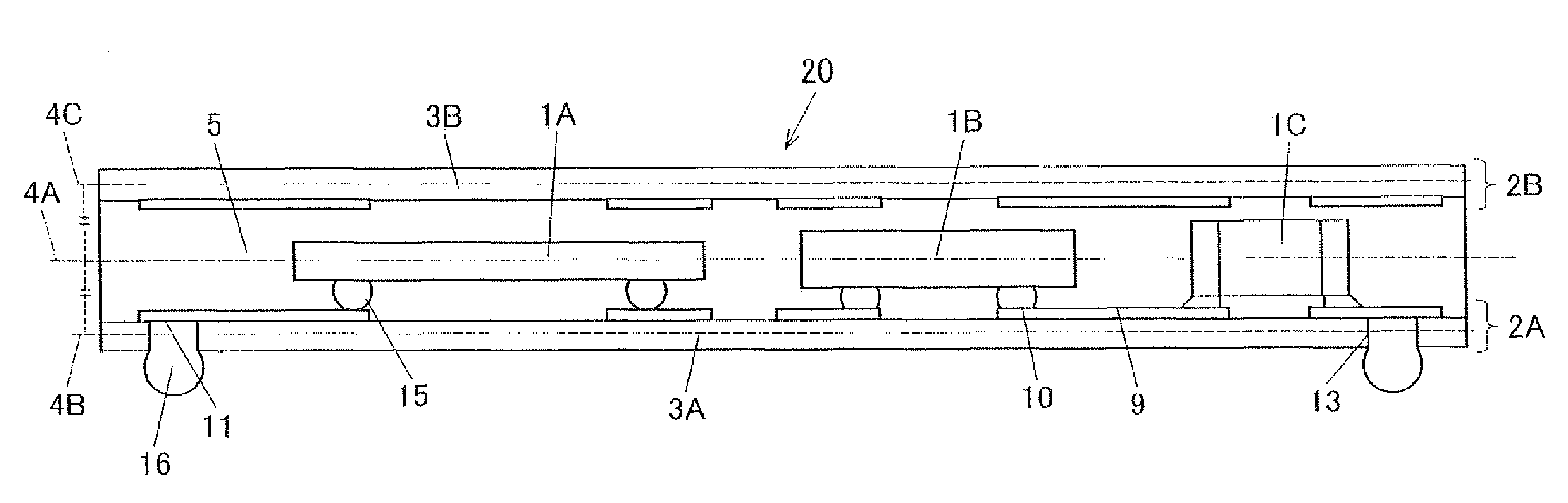
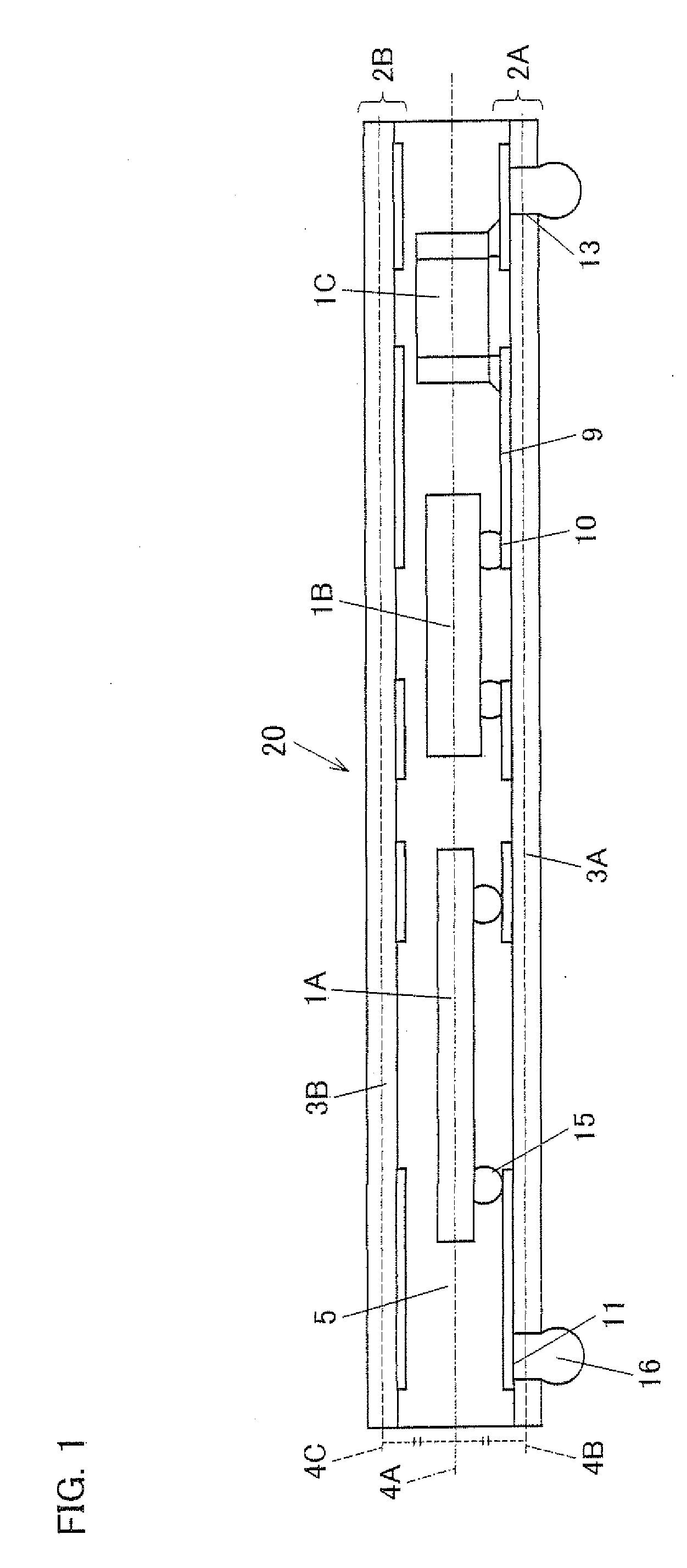
[0048]A multi-chip module of the present embodiment will be explained with reference to FIG. 1.

[0049]FIG. 1 is a cross section of the multi-chip module of the present embodiment.

[0050]The multi-chip module 20 shown in FIG. 1 includes an electronic component 1A, an electronic component 1B, and an electronic components 1C (i.e. bodies of electronic components) which are disposed in plane. The electronic component 1A and the electronic component 1B are active components including ICs and having different body sizes (i.e. different in planar size and thickness of each body). The electronic component 1C is a passive component having a different body size from the 1C components 1A and 1B. In the present embodiment, the electronic component 1A, electronic component 1B, and electronic component 1C are IC chips and a chip capacitor. The present invention, however, is not limited to this arrangement.

[0051]The body sizes of the electronic component 1A, electronic component 1B, and electronic c...

embodiment 21

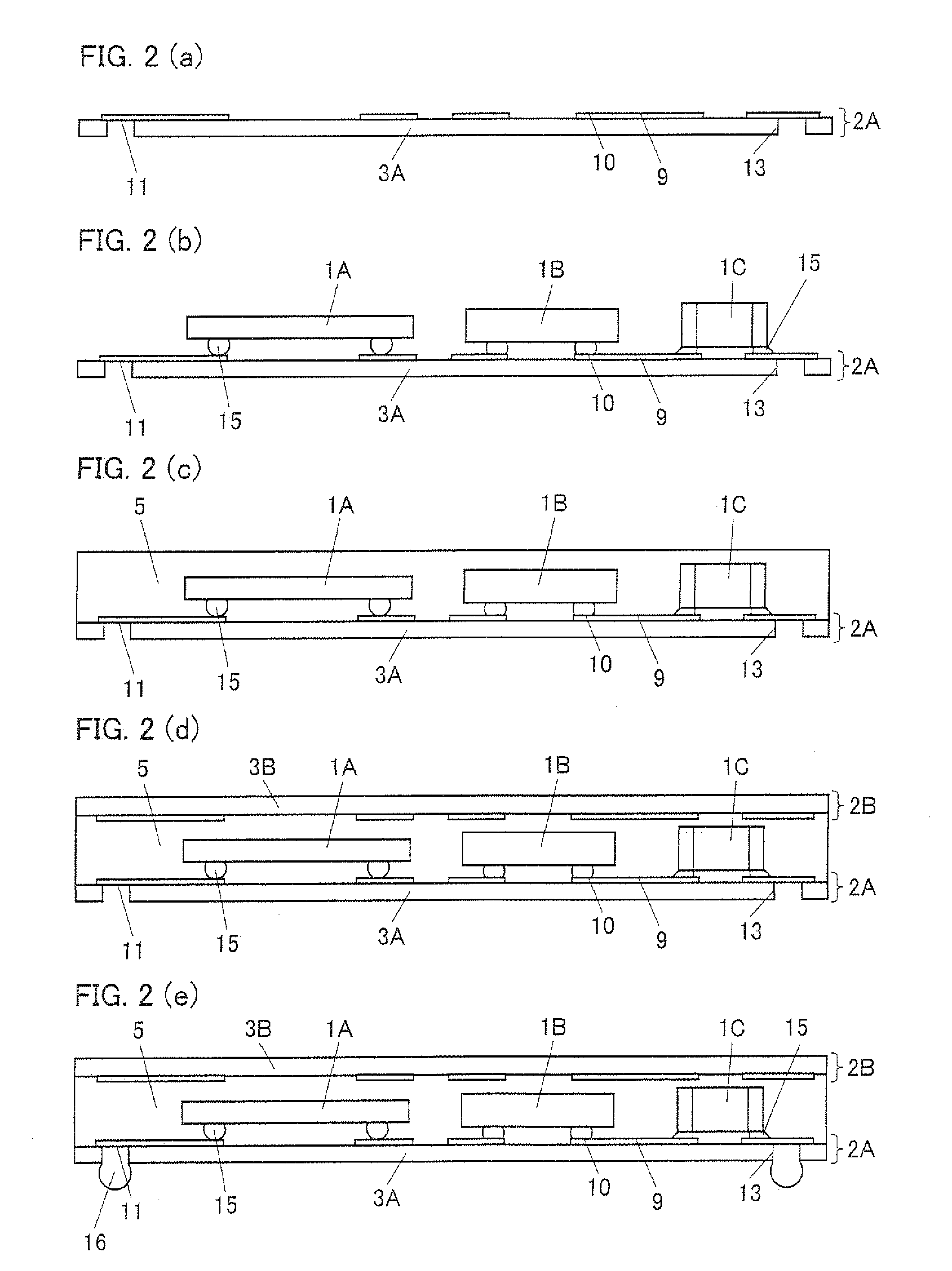
[0121]The following will explain a multi-chip module of the present embodiment with reference to FIG. 5.

[0122]FIG. 5 shows a horizontal cross section of the multi-chip module of the present embodiment. The multi-chip module of FIG. 5 is different from the multi-chip module of FIG. 1 in that there are three bases 3A, 3B, and 3C (all of them are 0.15 mm in thickness, for example) and four layers of wirings 9 (each of which is 0.02 mm in thickness, for example). Also, the wirings 9 are electrically connected to one another by wirings 8.

[0123]The number of layers of the bases and the number of layers of the wirings 9 are not particularly limited, and the number of layers can be arbitrarily determined. The warpage of the multi-chip module is reduced by arranging the bases 3A, 3B, 3C and so on and the bodies of the electronic components 1A, 1B, 1C, and so on are disposed in a substantially plane symmetrical manner with respect to the central plane of the multi-chip module 20.

[0124]In the ...


PUM


Abstract

With respect to the central plane which horizontally cuts a multi-chip module, constituent materials of the same type are disposed in a plane symmetrical manner. Each of an upper structure and a lower structure, which sandwich the central plane which horizontally cuts the multi-chip module, includes a base and electronic components, as the aforesaid constituent materials.

Description

[0001]This Nonprovisional application claims priority under 35 U.S.C. § 119(a) on Patent Application No. 345015 / 2006 filed in Japan on Dec. 21, 2006, the entire contents of which are hereby incorporated by reference.FIELD OF THE INVENTION[0002]The present invention relates to a multi-chip module constituted by plural components (such as an electronic component, a substrate, and wiring), a mounting structure of the multi-chip module, and a manufacturing method thereof.BACKGROUND OF THE INVENTION[0003]There have been proposed multi-chip modules in each of which plural semiconductor chips are mounted at the central part of a silicon substrate for the purpose of reduction in planar size, and column-shaped electrodes are provided around the outer periphery of the upper surface of the silicon substrate (e.g. Patent Document 1 (Japanese Laid-Open Patent Application No. 2001-94033; published on Apr. 6, 2001).[0004]For example, as shown in FIG. 10 the conventional multi-chip module 120 inclu...

Claims


Application Information

Patent Timeline
Patent Type & Authority Applications(United States)
IPC IPC(8): H01L23/552
CPCH01L23/5389H01L23/552H01L2924/07802H01L2924/10253H01L2225/06558H01L2224/48227H01L2224/48095H01L25/0655H01L2924/01078H01L2924/01079H01L2924/15311H01L2924/19041H01L2924/19105H01L2924/3025H05K1/185H01L24/48H01L2224/16225H01L2224/16227H01L2924/00014H01L2924/00H01L2224/451H01L2224/45147H01L24/45H01L2924/181H01L2924/14H01L2224/32145H01L2224/73265H01L2924/3511H01L2924/15321H01L2924/00012
Inventor ISHIO, TOSHIYA
Owner SHARP KK
Why Eureka
Try Eureka