
Image processing device

Inactive Publication Date: 2008-06-26
PANASONIC CORP
View PDF3 Cites 10 Cited by
  • Summary
  • Abstract
  • Description
  • Claims
  • Application Information

AI Technical Summary

Benefits of technology

[0007]The main object of the present invention therefore is to avoid deteriorations of the picture quality by preventing blurring of the contour generated at the boundary between the low-gradation area and the high-gradation area, which is caused because of pseudo multi-gradation processing.

Problems solved by technology

As a result, uniformity of the gradations cannot be maintained, thereby generating blurring of the contour at the boundary.
This may induce deteriorations of the picture quality.

Method used


Image

  • Image processing device
  • Image processing device
  • Image processing device

Examples


first embodiment

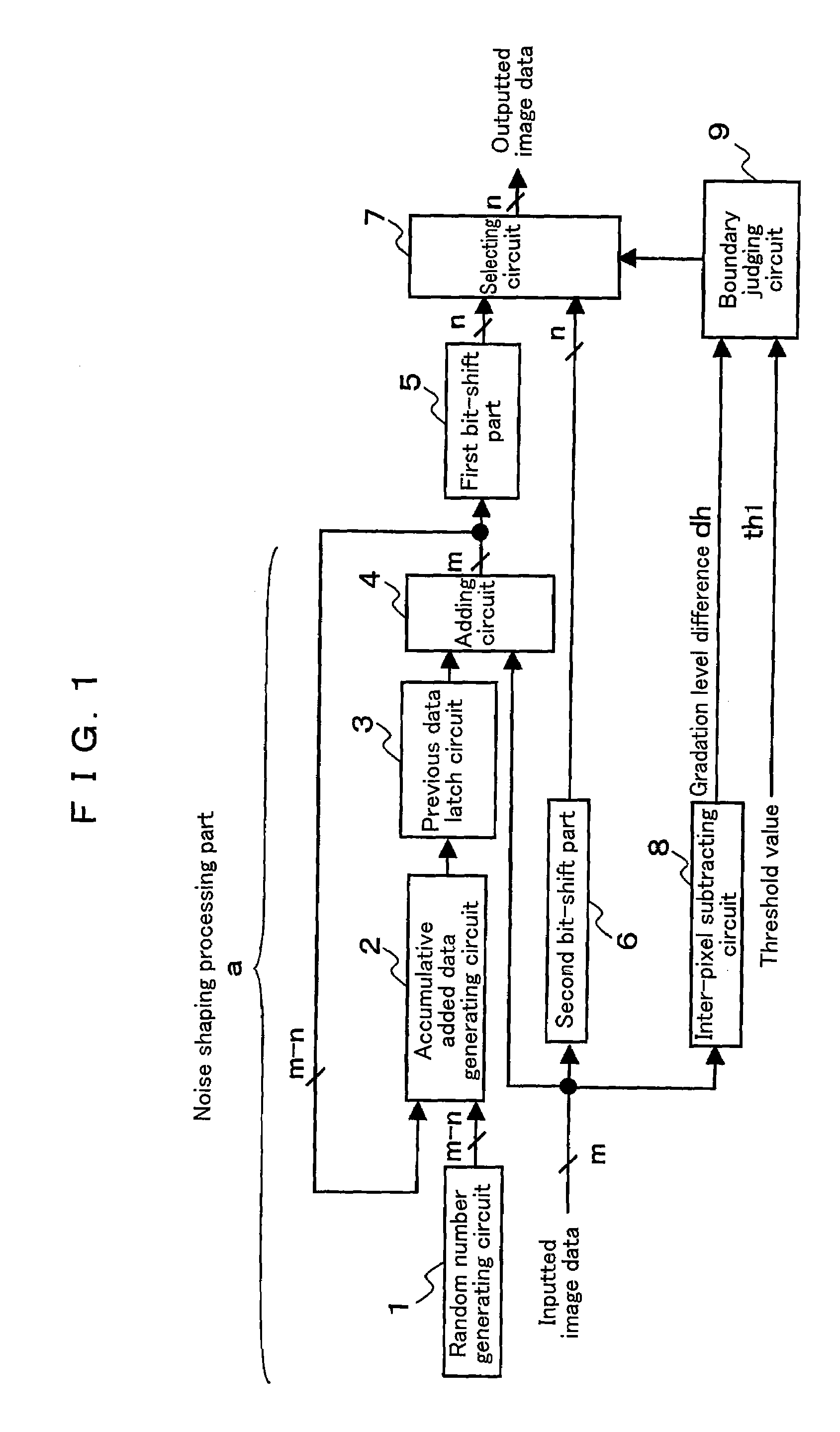
[0040]FIG. 1 is a block diagram for showing a structure of an image processing device according to a first embodiment of the present invention. In FIG. 1, reference code a is a noise shaping processing part. The noise shaping processing part a comprises a random number generating circuit 1, an accumulative added data generating circuit 2, a previous data latch circuit 3, and an adding circuit 4. The noise shaping processing part a performs accumulative adding operation on inputted pixel data for performing noise shaping processing. The accumulative added data generating circuit 2 generates accumulative added data from data of a lower (m-n)-bit pixel data generated by the adding circuit 4 and a random number value of (m-n)-bit generated by the random number generating circuit 1. The previous data latch circuit 3 holds the accumulative added data that is outputted from the accumulative added data generating circuit 2. The adding circuit 4 adds m-bit pixel data that is inputted from ou...

second embodiment

[0048]A second embodiment of the present invention is the same as the first embodiment, except that the second embodiment further calculates the number of continuous pixels of a same gradation in the horizontal direction and judges, based on the calculated number of continuous pixels of the same gradation, whether or not the boundary between the low-gradation area and the high-gradation area in the horizontal direction is a contour. Then, ON / OFF action of the accumulative adding processing is controlled in accordance with a result of the judgment.

[0049]FIG. 3 is a block diagram for showing a structure of an image processing device according to the second embodiment of the present invention. In FIG. 3, same reference numerals as those of FIG. 1 showing the first embodiment indicate the same structural elements.

[0050]Reference numeral 10 is a contour judging circuit. The contour judging circuit 10 performs the followings.[0051]Processing for comparing the gradation level difference dh...

third embodiment

[0066]A third embodiment of the present invention judges presence of a boundary on the basis of a gradation level difference dv between the neighboring pixels in the vertical direction, whereas the first embodiment judges the presence of the boundary on the basis of the gradation level difference dh between the neighboring pixels in the horizontal direction.

[0067]FIG. 6 is a block diagram for showing a structure of an image processing device according to the third embodiment. In FIG. 6, the same reference numerals as those of FIG. 1 according to the first embodiment indicate the same structural elements. Reference numeral 3a is a line memory for storing output error data of the accumulative added data generating circuit 2 for one horizontal period, and 3b is a line memory for storing inputted pixel data for one horizontal period. In this embodiment, the adding circuit 4 adds, by each line, pixel data of m-bits inputted from outside and output error data of (m-n)-bit supplied from th...


PUM


Abstract

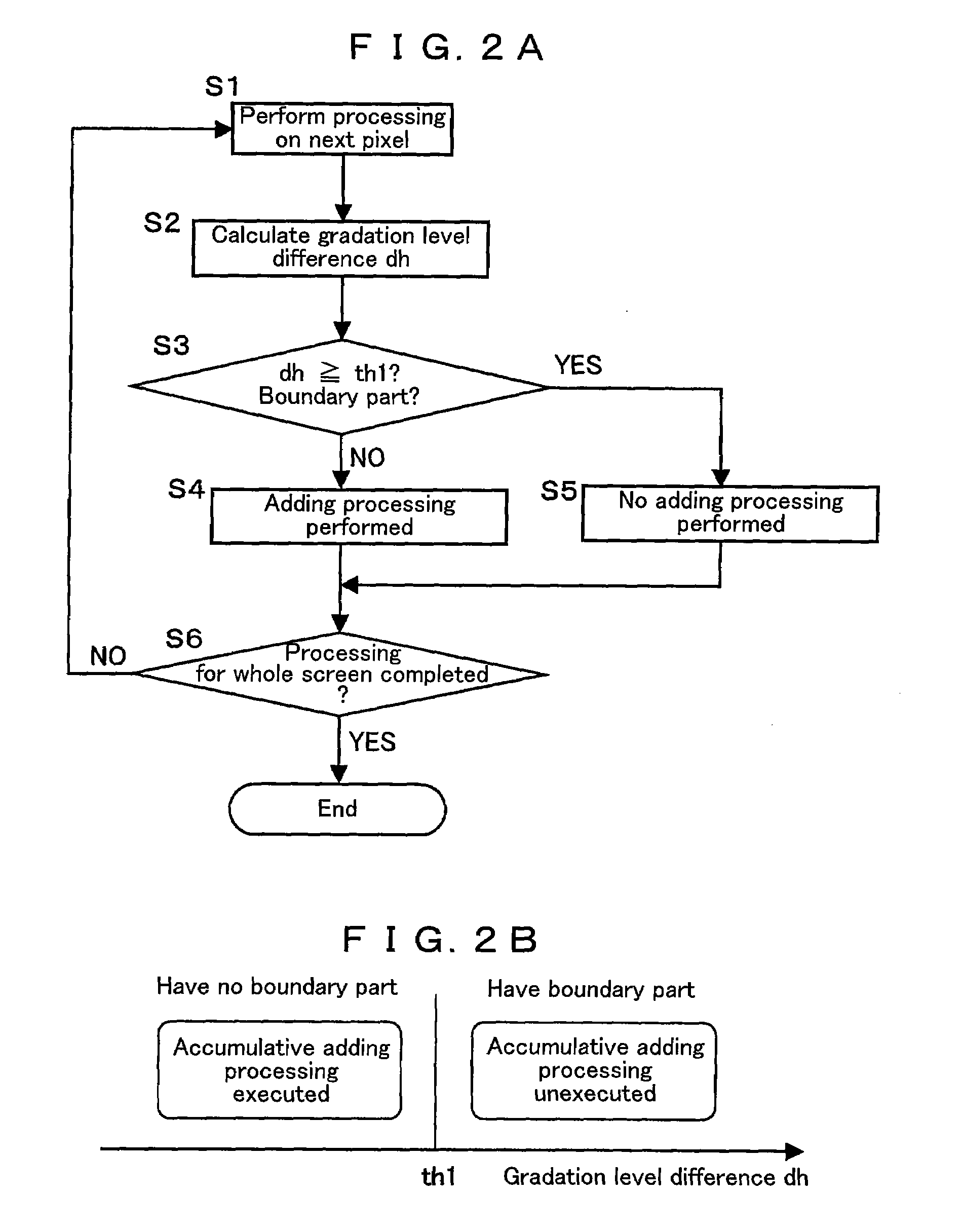
A noise shaping processing part performs noise shaping processing on pixel data. An adding circuit performs accumulative adding processing on the noise-shaped pixel data. A first bit-shift part performs bit-shift processing on the accumulatively-added and noise-shaped pixel data. A second bit-shift part performs bit-shift processing on unprocessed pixel data. An inter-pixel subtracting circuit calculates a gradation level difference between neighboring current pixel and previous pixel in a horizontal direction in the unprocessed pixel data. A boundary judging circuit judges presence of a boundary between a low-gradation area and a high-gradation area in the horizontal direction of the unprocessed pixel data, based on a comparison between the gradation level difference and a prescribed threshold value. A selecting circuit selects an output of the first bit-shift part when the boundary judging circuit judges there is no boundary, and selects an output of the second bit-shift part when judged there is a boundary.

Description

BACKGROUND OF THE INVENTION[0001]1. Field of the Invention[0002]The present invention relates to an image processing device which performs pseudo multi-gradation processing on pixel data (mainly color images).[0003]2. Description of the Related Art[0004]Conventionally, as pseudo multi-gradation processing such as color reduction processing performed on pixel data, known is a noise shaping technique which, when a bit precision of an output device is lower than the number of bits of inputted pixel data, discards information of a lower bit of the pixel data so as to be suited for the bit precision of the output device.[0005]FIG. 10 shows a structure of accumulative adding processing performed in a typical noise shaping technique. An accumulative added data generating circuit 2 generates accumulative added data from data of a lower (m-n)-bit of pixel data generated by an adding circuit 4 and a random number value of the (m-n)-bits generated by a random number generating circuit 1, and h...

Claims


Application Information

Patent Timeline
IPC IPC(8): H04N5/217G06T5/00H04N1/405
CPCG06T2207/10016G06T2207/20012G06T5/002G06T2207/20192G06T5/70
Inventor OSAKA, NAOTOKUNITANI, HISAOITOMAN, TATUO
Owner PANASONIC CORP
Learn More