Real-time fault detection and classification system in use with a semiconductor fabrication process

a real-time fault detection and classification system technology, applied in the field of semiconductor fabrication process, can solve the problems of poor product yield, poor fault detection and classification system workers, and only achieving the equipment efficiency of semiconductor manufacturers, so as to increase the product yield of the semiconductor fabrication process

Active Publication Date: 2008-06-26
IND TECH RES INST
View PDF21 Cites 13 Cited by
  • Summary
  • Abstract
  • Description
  • Claims
  • Application Information

AI Technical Summary

Benefits of technology

[0008]According to the above drawbacks, an objective of the present invention is to provide a fault detection and classification (FDC) system in use with a semiconductor fabrication process for increasing product yield of the semiconductor fabrication process.

Problems solved by technology

However, according to an estimation of the Semiconductor Manufacturing Technology Consortium (SEMATECH), equipment efficiency of semiconductor manufacturers only reaches 40-50%.
Therefore, workers on the fault detection and classification system 1 cannot timely maintain the semiconductor tool 13 or the facility monitoring control system 14.
Accordingly, semiconductor fabrication processes using the conventional fault detection and classification system 1 can result in a poor product yield.

Method used


Image

  • Real-time fault detection and classification system in use with a semiconductor fabrication process
  • Real-time fault detection and classification system in use with a semiconductor fabrication process
  • Real-time fault detection and classification system in use with a semiconductor fabrication process

Examples


Embodiment Construction

[0013]The following illustrative embodiments are provided to illustrate the disclosure of the present invention, these and other advantages and effects can be apparent to those skilled in the art after reading the disclosure of this specification. The present invention can also be performed or applied by other different embodiments. The details of the specification may be on the basis of different points and applications, and numerous modifications and variations can be made without departing from the spirit of the present invention.

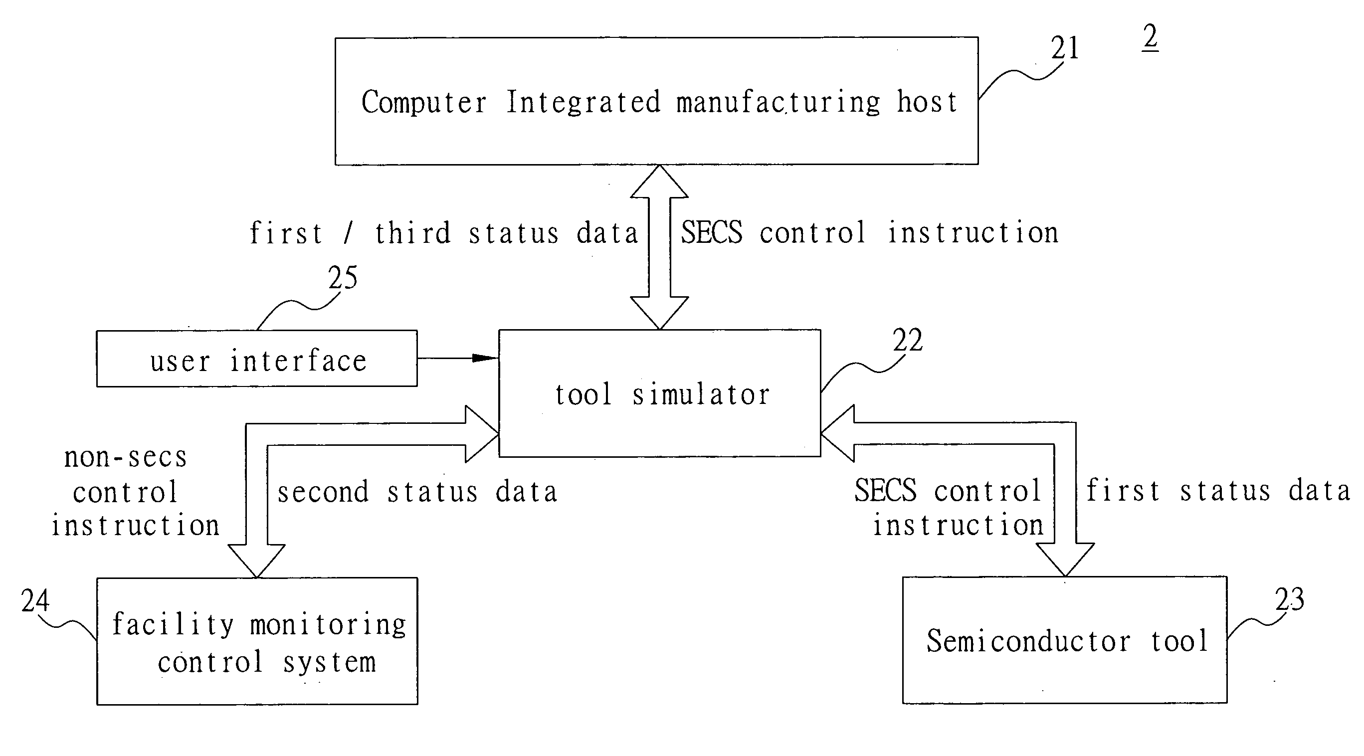
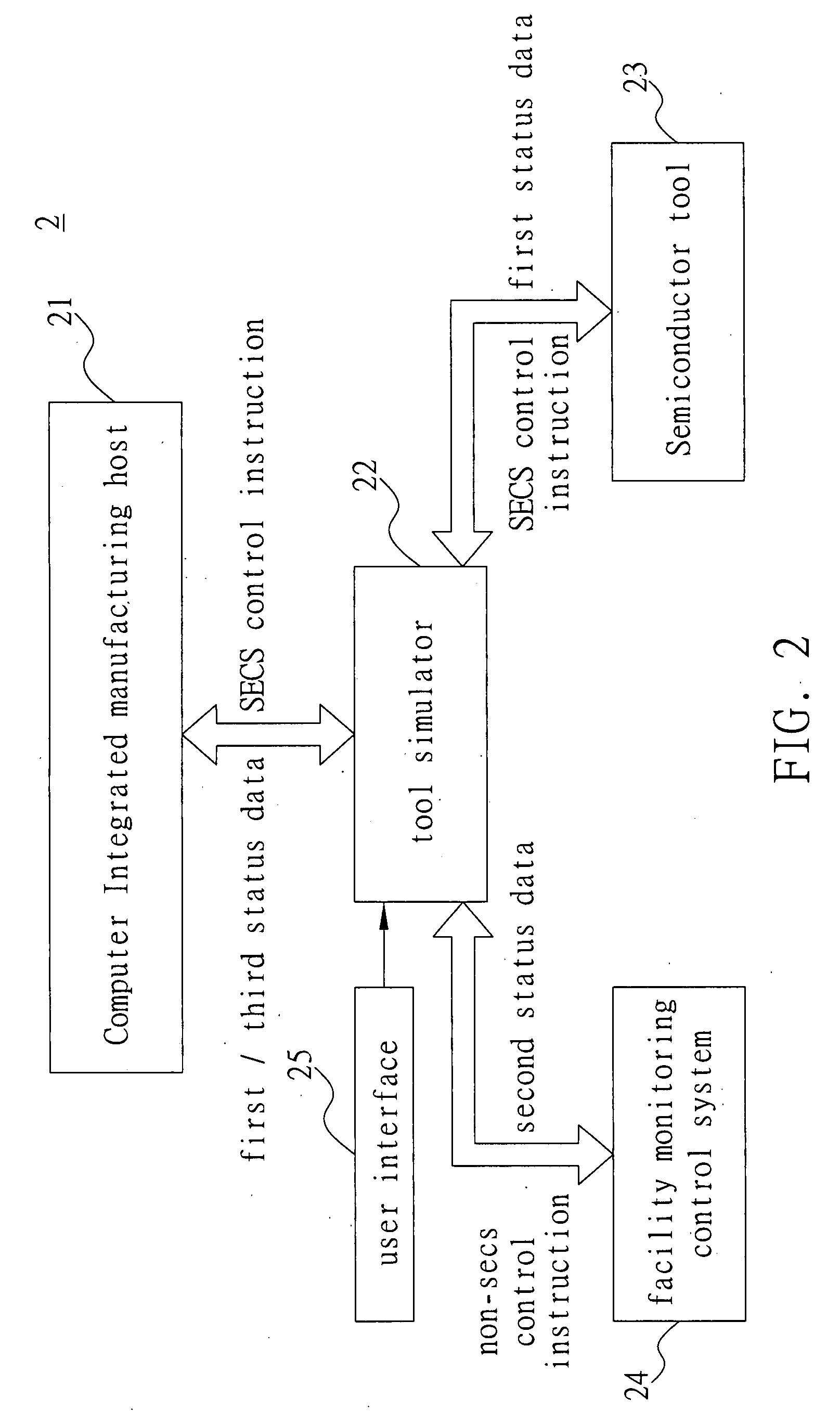
[0014]FIG. 2 is a block diagram of a real-time fault detection and classification system 2 in use with a semiconductor fabrication process according to a preferred embodiment the present invention, wherein the semiconductor fabrication process comprises a first sub-fabrication process and a second sub-fabrication process. The real-time fault detection and classification system 2 comprises a computer integrated manufacturing (CIM) host 21, a semiconductor...


PUM


Abstract

A real-time fault detection and classification (FDC) system, which is in use with a semiconductor fabrication process having a first sub-fabrication process and a second sub-fabrication process, includes a computer integrated manufacturing (CIM) host adopting a SEMI equipment communication standard (SECS), a semiconductor tool for executing the first sub-fabrication process and generating first status data in conformity with the SECS, a non-semiconductor tool for executing the second sub-fabrication process and generating second status data in conformity with a predetermined connectivity standard different from the SECS, and a tool simulator connecting the tool simulator with the semiconductor tool and the non-semiconductor tool for receiving the first and second status data and transforming the second status data into third status data in conformity with the SECS such that the CIM host can classify the first and third status data according to a predetermined classification technique and get a control over equipment health conditions of the semiconductor tool as well as the non-semiconductor tool.

Description

BACKGROUND OF THE INVENTION[0001]1. Field of the Invention[0002]The present invention relates generally to a semiconductor fabrication process, and more particularly to a real-time fault detection and classification system in use with a semiconductor fabrication process.[0003]2. Description of Related Art[0004]In order to keep competitive manufacturing ability, semiconductor manufacturers are decreasing manufacturing cost of semiconductor components by 25-30% each year. As pointed out by International Technology Roadmap for Semiconductors (ITRS), four possible methods for reducing manufacturing cost include reducing feature sizes, increasing wafer diameter, improving product yield and increasing overall equipment effectiveness (OEE). As to current semiconductor technology, increasing wafer diameter and improving product yield can at most reduce 3% of the manufacturing cost, and decreasing feature sizes can reduce about 12% to 14% of the manufacturing cost. However, according to an e...

Claims


Application Information

Patent Timeline
Patent Type & Authority Applications(United States)
IPC IPC(8): G06F19/00
CPCG05B19/4184G05B2219/45031G05B2219/32356Y02P90/02
Inventor CHANG, YI-CHUNPAO, CHAN-ANTSAI, CHENG-TSO
Owner IND TECH RES INST
Why Eureka
Try Eureka