Semiconductor device and method of manufacturing the same

a semiconductor device and semiconductor technology, applied in the direction of semiconductor devices, semiconductor/solid-state device details, electrical devices, etc., can solve the problems of reducing limiting the reduction of the height of the semiconductor device, and difficult to connect the wire stably, so as to minimize the damage to the side surface of the semiconductor element, improve the yield ratio of the semiconductor device, and minimize peeling

Active Publication Date: 2008-07-03
SPANSION LLC
View PDF14 Cites 23 Cited by
  • Summary
  • Abstract
  • Description
  • Claims
  • Application Information

AI Technical Summary

Benefits of technology

[0024]Mounting the built-in semiconductor device on the semiconductor element may include fixing the built-in semiconductor device directly on the semiconductor element. Fixing the built-in semiconductor device directly on the semiconductor element may include coating a fixing agent so that the fixing agent covers the upper surface of the semiconductor element. With this method, the fixing portion protects an interface between the side surface of the semiconductor device and the molding portion. It is therefore possible to minimize the peeling at an interface between the molding portion and the semiconductor element. Mounting the built-in semiconductor device may include mounting the built-in semiconductor device so that a space is formed between the semiconductor element and the built-in semiconductor device. With this method, it is possible to mount the built-in semiconductor device on the semiconductor device in which the entire side surface is covered with the molding portion and an upper surface is not covered with the molding portion. It is possible to minimize the damage to the side surface of the semiconductor element caused by an external impact, at any time before mounting the built-in semiconductor device or during the mounting of the built-in semiconductor device, because the entire side surface of the semiconductor element is covered with the molding portion. It is also possible to improve the yield ratio of the semiconductor device. Mounting the built-in semiconductor device on the semiconductor element may include coupling the semiconductor element to the built-in semiconductor device electrically with a bump. With this method, it is possible to connect the semiconductor element to the built-in semiconductor device with a small bump, because there is no molding portion on the semiconductor element. It is therefore possible to reduce the thickness of the semiconductor device. It is also possible to reduce an interval between the bumps in a lateral direction. As such, it is possible to reduce the size of the semiconductor device.

Problems solved by technology

Therefore, there is a limit to the reduction of the height of the semiconductor device.
It is difficult to connect the wire stably, and the yield ratio of the semiconductor device is reduced.
This results in an inferior semiconductor device.
Therefore, the risk of damaging the side surface of the semiconductor element 14 caused by an external impact increases in the previous mounting of the built-in semiconductor device 52.
However, there is the same problem as the case of the first conventional embodiment in the semiconductor device disclosed in Document 1, because the upper surface of the semiconductor element is enclosed by the molding portion.

Method used


Image

  • Semiconductor device and method of manufacturing the same
  • Semiconductor device and method of manufacturing the same
  • Semiconductor device and method of manufacturing the same

Examples


fourth embodiment

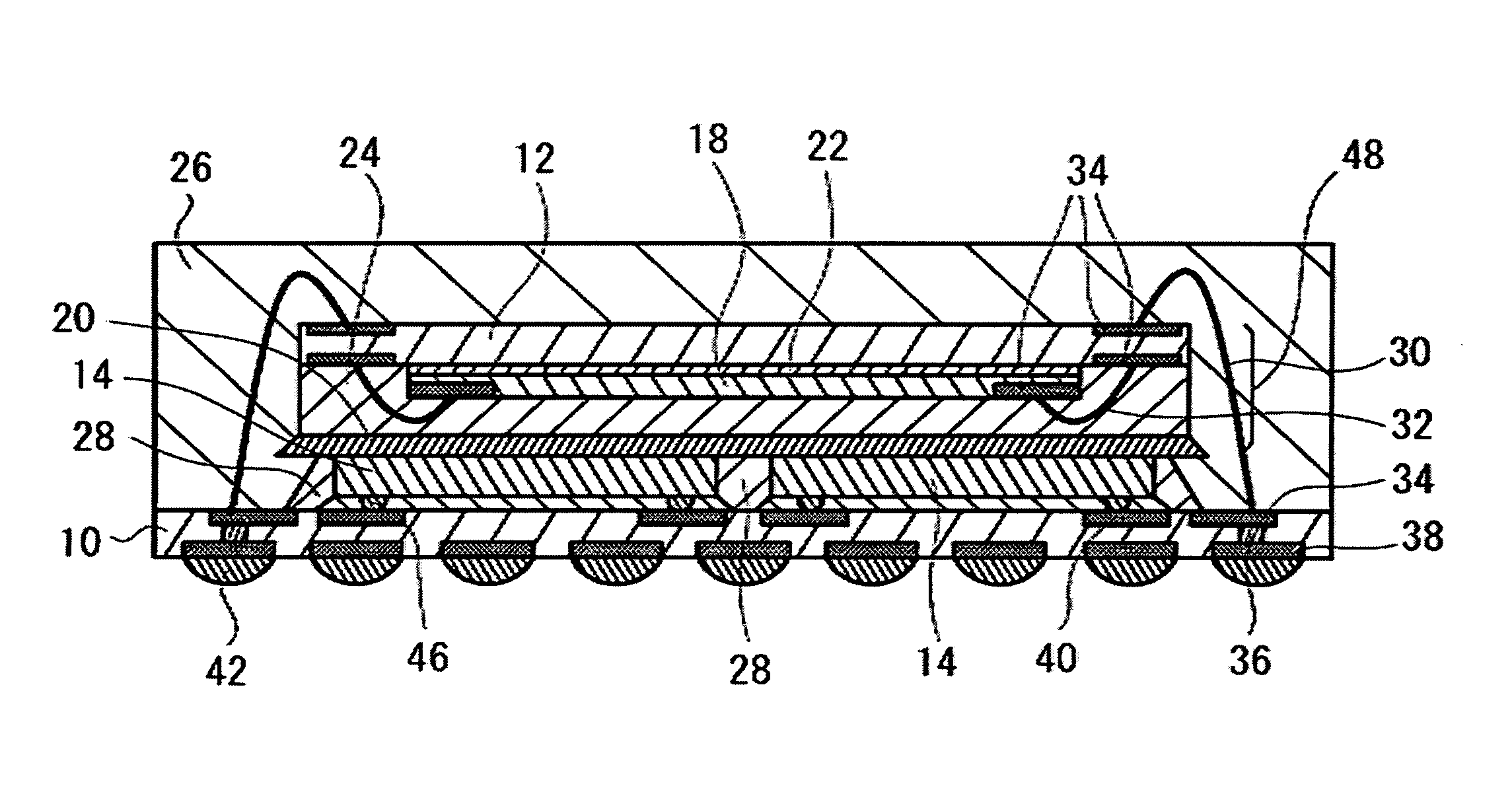
[0051]As shown in FIG. 7 and FIG. 8, in a semiconductor device in accordance with the fourth embodiment, the entire upper surface of the semiconductor element 14 is covered with the fixing portion 20. It is therefore possible to minimize the peeling of the molding portion 28 from the side surface of the semiconductor element 14 because the fixing portion 20 protects the interface between the side surface of the semiconductor element 14 and the molding portion 28. It is also possible to improve the yield ratio of the semiconductor device.

[0052]As shown in FIG. 8, a region of the upper surface of the semiconductor element 14 where the built-in semiconductor device 48 is projected is inside of the upper surface of the semiconductor element 14. In other words, the built-in semiconductor device 48 is not in contact with the molding portion 28, and is directly fixed only to the upper surface of the semiconductor element 14 through the fixing portion 20. With this structure, it is possible...

fifth embodiment

[0055]Further, in the process shown in FIG. 9C, the molding portion 28 does not enclose the upper surface of the semiconductor element 14. That is, the built-in semiconductor device 48 is not in contact with the molding portion 28, and is directly fixed only to the upper surface of the semiconductor element 14. Generally, the thermal conductivity of the epoxy resin composing the molding portion 28 is lower than that of silicon composing the semiconductor element 14. It is therefore possible to conduct the heat from the substrate 10 to the built-in semiconductor device 48 at a maximum level, because the heat from the substrate 10 is conducted to the built-in semiconductor device 48 via the semiconductor element 14 and the fixing portion 20 when the substrate 10 is coupled to the substrate 12 with the wire 30. It is therefore possible to stably couple the built-in semiconductor device 48 to the substrate 10 with the wire. As such, it is possible to improve the yield ratio of the semic...


PUM


Abstract

The present invention provides a semiconductor device with an improved yield ratio and reduced height and manufacturing cost; and a method of manufacturing the semiconductor device. According to an aspect of the present invention, there is provided a semiconductor device including a substrate, a semiconductor element that is flip-chip connected to the substrate, and a molding portion that seals the semiconductor element. The side surfaces of the semiconductor element are enclosed by the molding portion. An upper surface of the semiconductor element is not enclosed by the molding portion. Damage to the side surfaces of the semiconductor element caused by an external impact when the semiconductor device is stored is minimized, because the molding portion protects the side surfaces of the semiconductor element. Accordingly, the yield ratio of the semiconductor device is improved. The height of the semiconductor device can also be reduced since the upper surface of the semiconductor element is not enclosed with the molding portion.

Description

CLAIM OF PRIORITY[0001]This is a continuation-in-part of International Application No. PCT / JP 2006 / 353411, filed Dec. 27, 2006 which was not published in English under PCT Article 21(2).TECHNICAL FIELD[0002]This invention generally relates to a semiconductor device and a method of manufacturing the semiconductor device, and in particular, relates to a semiconductor device in which a plurality of built-in semiconductor devices are stacked and a method of manufacturing the semiconductor device.BACKGROUND OF THE INVENTION[0003]Recently, there has been a demand for downsizing a semiconductor device that is used for a portable electronic device such as a mobile phone or a nonvolatile record media of an IC memory card. As such, there is a demand for packaging a semiconductor element efficiently. There exists an art in which a semiconductor element is stacked and is packaged.[0004]A description will be given of a first through third conventional embodiments as an example of the art where t...

Claims


Application Information

Patent Timeline
Patent Type & Authority Applications(United States)
IPC IPC(8): H01L23/48H01L21/56
CPCH01L2224/16225H01L2224/32145H01L2224/32225H01L2224/48227H01L2224/73204H01L2224/73253H01L2224/73265H01L2924/15311H01L2924/15331H01L2924/18161H01L2924/19107H01L23/3128H01L23/3135H01L24/48H01L25/0652H01L25/105H01L2224/48091H01L2224/73203H01L2225/1023H01L2225/1052H01L2225/1058H01L2924/01079H01L24/73H01L2924/14H01L2924/00014H01L2224/45144H01L24/45H01L2924/00011H01L21/563H01L2924/00012H01L2924/00H01L2224/0401H01L2224/45015H01L2924/207H01L25/0657H01L25/50H01L2224/48228
Inventor ONODERA, MASANORI
Owner SPANSION LLC
Why Eureka
Try Eureka