Semiconductor memory device with mirror function module and using the same

a memory device and mirror function technology, applied in the field of mirror function modules and memory devices of semiconductors, can solve problems such as deteriorating the setup/hold performance of signals, and achieve the effect of preventing skews

Inactive Publication Date: 2008-07-03
SK HYNIX INC
View PDF4 Cites 73 Cited by
  • Summary
  • Abstract
  • Description
  • Claims
  • Application Information

AI Technical Summary

Benefits of technology

[0012]It is an object of the present invention to solve the delay difference generated between the signals transferred to mirror function “on” paths and mirror function “off” path “off” paths generated in a package with a mirror function, and to prevent skew occurrence between the signals.

Problems solved by technology

The resulting skew generates the difference between a setup / hold time forming a window of the signal, thereby deteriorating the setup / hold performance of the signal.

Method used


Image

  • Semiconductor memory device with mirror function module and using the same
  • Semiconductor memory device with mirror function module and using the same
  • Semiconductor memory device with mirror function module and using the same

Examples


Embodiment Construction

[0033]Hereinafter, preferred embodiments of the present invention will be described in detail with reference to the accompanying drawings.

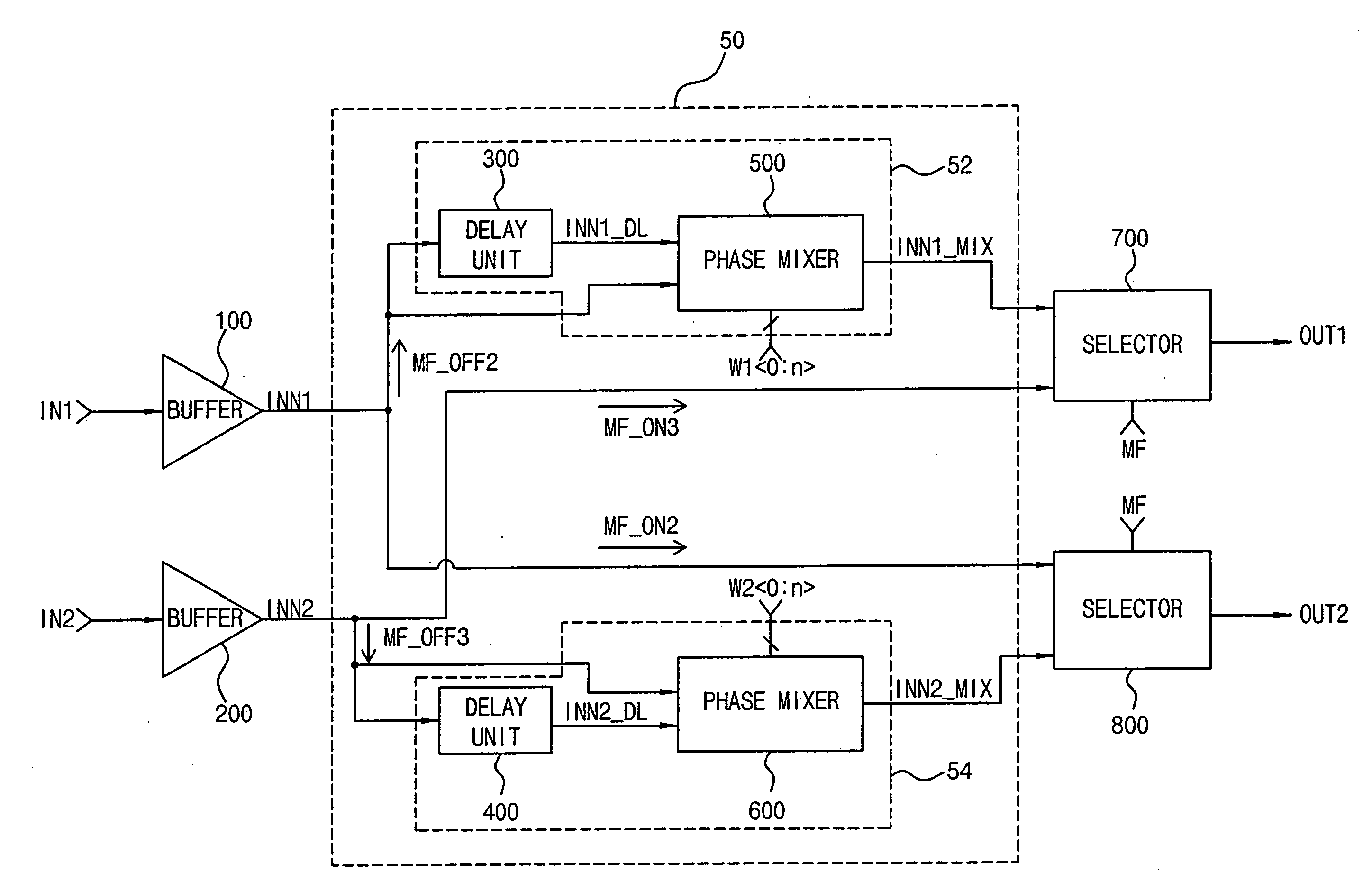
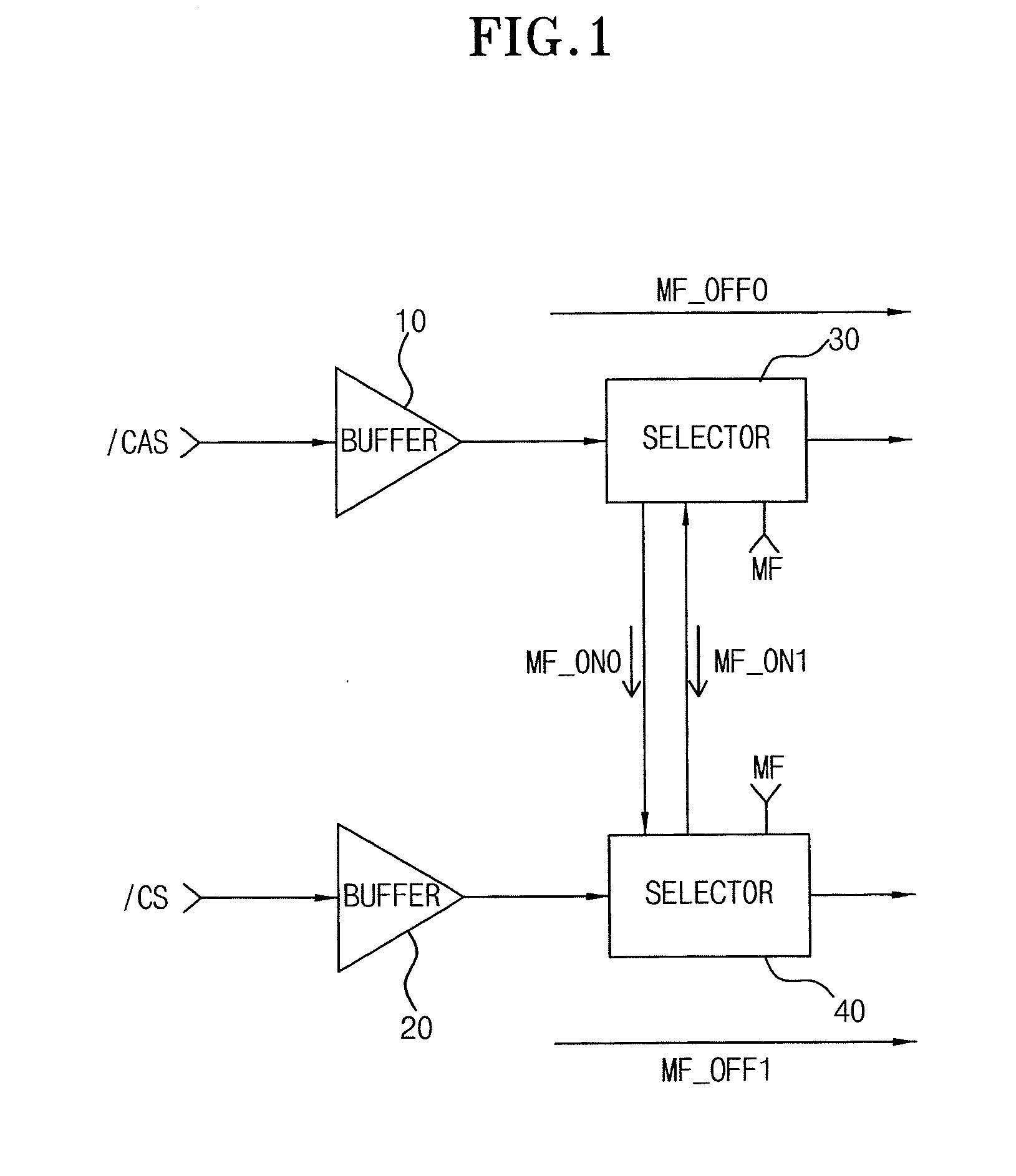
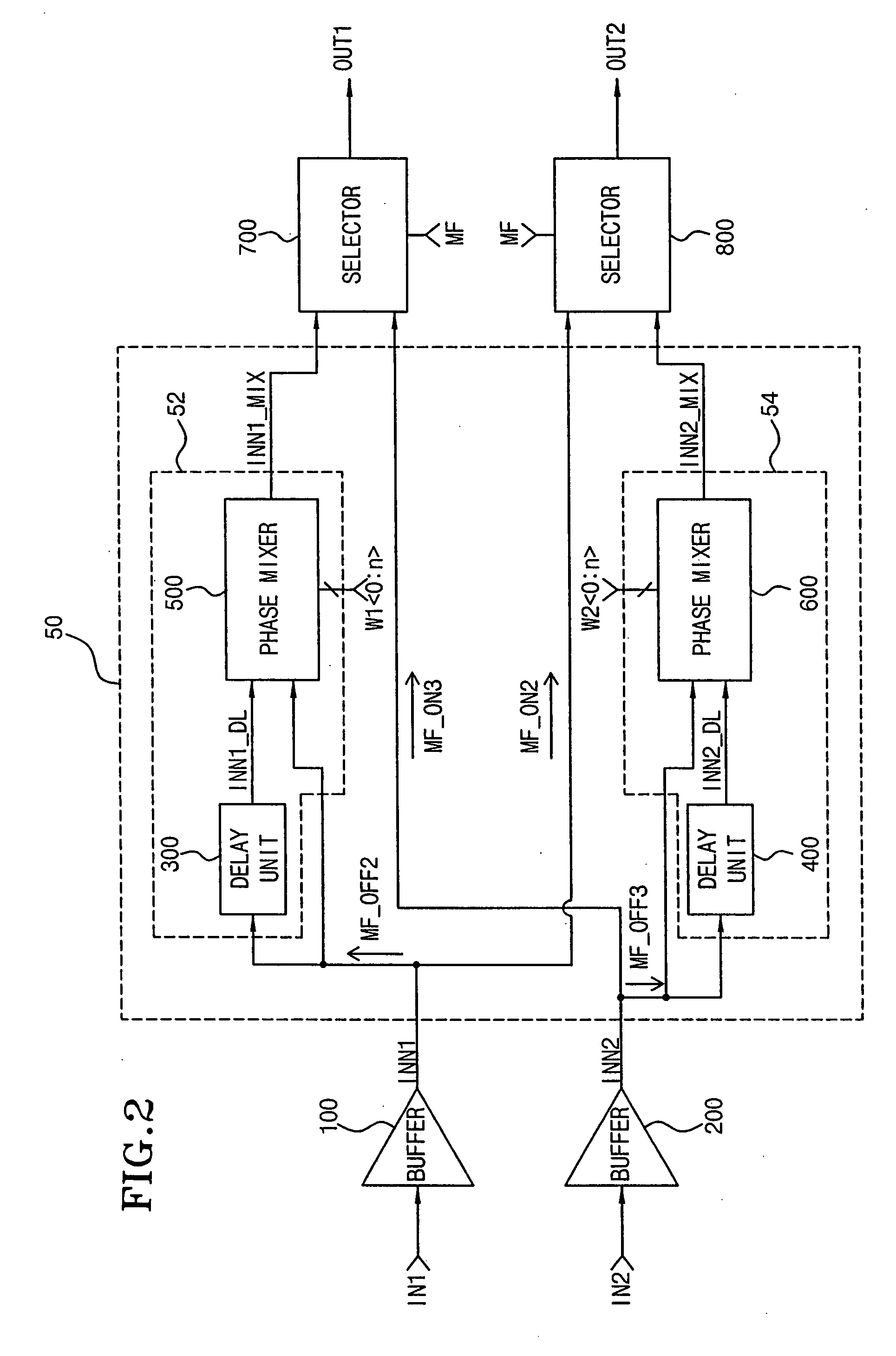
[0034]The present invention can be applied to a memory module mounted with at least a pair of semiconductor memory devices on opposing sides of a substrate such that contacts or leads of the pair of semiconductor memory devices are symmetrical to each other to allow inputting a first transmission signal and second transmission signal used in common to the pads arranged to be symmetrical to each other and providing a mirror function that the first transmission signal and the second transmission signal input to the respective pads are transferred to any one of a mirror “on” path and a mirror “off” path “off” path for itself.

[0035]The semiconductor memory device mounted on the module can be formed of DRAMs, each DRAM providing the mirror function, delaying the transmission signals to be identical or similar to each other on a mirror function “on” pat...


PUM


Abstract

A semiconductor memory device with a mirror function enables two memory devices such as two DRAMs to share the same address and control signals. A pair of semiconductor memory devices are mounted on both sides of a substrate to be symmetrical to each other. A mirror function transfers a first transmission signal and a second transmission signal input on respective pads to any one of a mirror “on” path and a mirror “off” path. The mirror function can vary or reduce path delay differences between the mirror function “on” path and the mirror function “off” path by means of the delay and the mixture of phases in the semiconductor memory device, and reduce skew occurred in the operation of the mirror function.

Description

CROSS-REFERENCE TO RELATED APPLICATIONS[0001]The present application claims priority to Korean patent application number 10-2006-0137166 filed on Dec. 28, 2006, which is incorporated herein by reference in its entirety.BACKGROUND OF THE INVENTION[0002]The present invention relates to a semiconductor device, and more particularly to a semiconductor memory device with a mirror function and a module mounting thereof.[0003]In general, a dynamic random access memory or DRAM is typically manufactured in a module as a so-called Double In-line Memory Module (DIMM) or a module with a shape where DRAM device is mounted on both sides of a substrate.[0004]DIMM modules mounted with DRAM on both sides of a substrate generally have DRAMs that both use the same signal lines, such as the address and control lines in common with each other. The pin (pad) to which commonly used signals (for being used in common by DRAM packages on both sides of the substrate) should be arranged so that they are symmet...

Claims


Application Information

Patent Timeline
Patent Type & Authority Applications(United States)
IPC IPC(8): G11C7/00
CPCG11C7/109G11C7/1078G11C11/407G11C11/4091G11C11/4093
Inventor KIM, YOUNG JU
Owner SK HYNIX INC
Why Eureka
Try Eureka