Synchronous semiconductor memory device

Active Publication Date: 2008-07-10
NVIDIA CORP
View PDF9 Cites 7 Cited by
  • Summary
  • Abstract
  • Description
  • Claims
  • Application Information

AI Technical Summary

Benefits of technology

[0021]As described above, according to the present invention, when using the internal clocks into which the external clock is divided to count the set latency, the latency counter including the first counter circuit and the second counter circuit is provided so as to form a signal path which is shifted therebetween, and therby various latencies can be selectively counted regardless of whether the number is even or odd. And when using the high-speed external clock, the latency coun

Problems solved by technology

Further, with progress of the DDR-SDRAM generation, speed of the external clock increases and the required latency tends to gradually increase.
That is, since the internal clock having the same frequency as the external clock is applied to each stage of the nine-stage shift register, sequential shift operation of each stage performed at every period tCK of the external clock causes a problem of an

Method used


Image

  • Synchronous semiconductor memory device
  • Synchronous semiconductor memory device
  • Synchronous semiconductor memory device

Examples


Example

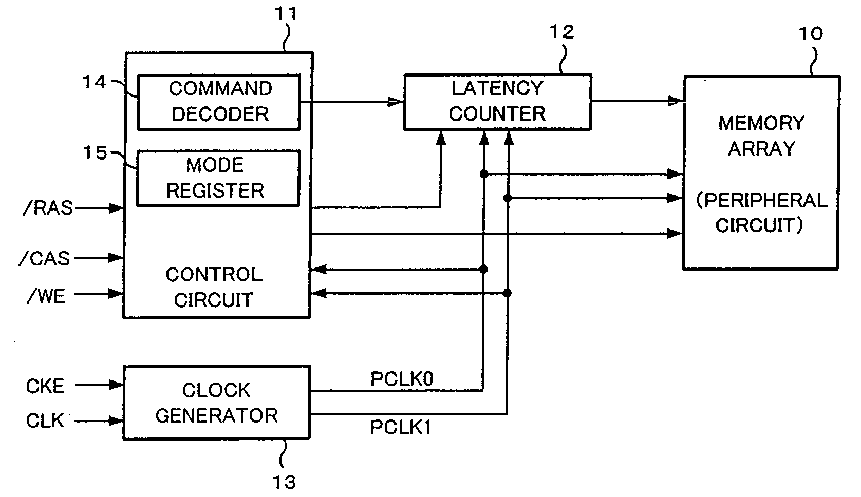
[0035]Embodiments of the present invention will be described hereinafter with reference to accompanying drawings. In this embodiment, a synchronous semiconductor memory device to which the present invention applied is, for example, a DDR-SDRAM having a latency counter for counting latencies set for various commands.

[0036]FIG. 1 is a block diagram showing a principal configuration of a synchronous semiconductor memory device of this embodiment. The synchronous semiconductor memory device as shown in FIG. 1 includes a memory array 10, a control circuit 11, a latency counter 12, and a clock generator 13. Actually the synchronous semiconductor memory device includes many other components, but only components related to the function based on the present invention are shown in FIG. 1.

[0037]In the above-mentioned configuration, the memory array 10 includes a plurality of memory cells formed at intersections of a plurality of word lines and a plurality of bit lines arranged in a matrix, and...


PUM


Abstract

A synchronous semiconductor memory device of the present invention has a clock generator for generating a normal and a reverse phase clocks by dividing an external clock, a command decoder for decoding an external command and outputting a command signal; latency setting means capable of selectively setting an even or odd number latency within a range of a predetermined number of clock cycles of the external clock, a latency counter which includes two counter circuits for sequentially shifting the command signal captured using the normal and reverse phase clock and being capable of switching a signal path in response to the number of clock cycles, and first and second control means which controls counting of the clock cycles equivalent to the even or odd number latency by forming an appropriate signal path.

Description

BACKGROUND OF THE INVENTION[0001]1. Field of the Invention[0002]This invention relates to a synchronous semiconductor memory device which operates in synchronization with a clock, and particularly relates to a synchronous semiconductor memory device having a configuration for controlling operation timings corresponding to a latency after an issuance of a command for various purposes.[0003]2. Description of the Related Art[0004]Recently SDRAM (Synchronous Dynamic Random Access Memory) of DDR (Double Data Rate) type has been a mainstream as a synchronous semiconductor memory device to allow high speed operation. Since this DDR-SDRAM (referred to as DDR-SDRAM hereinafter) employs a high speed clock, a considerable number of clock cycles are required between issuing a command and completion of a data transmission in read / write operation. Therefore, a configuration is employed in which a predetermined number of clock cycles of an external clock is preliminarily set as a latency based on ...

Claims


Application Information

Patent Timeline
IPC IPC(8): G11C8/00
CPCG11C7/22G11C11/4076G11C7/222
Inventor FUJISAWA, HIROKIKUBOUCHI, SHUICHIKUROKI, KOJI
Owner NVIDIA CORP
Why Eureka
Try Eureka