Image display device

Inactive Publication Date: 2006-11-30
HITACHI LTD
View PDF8 Cites 3 Cited by
  • Summary
  • Abstract
  • Description
  • Claims
  • Application Information

AI Technical Summary

Benefits of technology

[0018] According to the embodiment of the present invention, an image display device

Problems solved by technology

Furthermore, trouble of heating the panel due to Jo

Method used


Image

  • Image display device
  • Image display device
  • Image display device

Examples


embodiment 1

[0034] In this embodiment, a description is made using the passive-matrix-drive FED as an example, which has MIM (Metal-Insulator-Metal) electron sources as the electron emission elements. However, embodiments of the present invention can be applied similarly to an FED having electron sources other than the MIM electron sources, for example, SCE (surface conduction electron-emitter) or carbon-nano-tube electron sources.

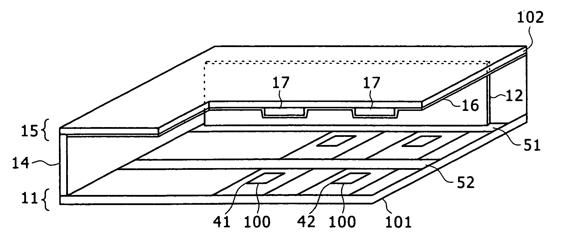
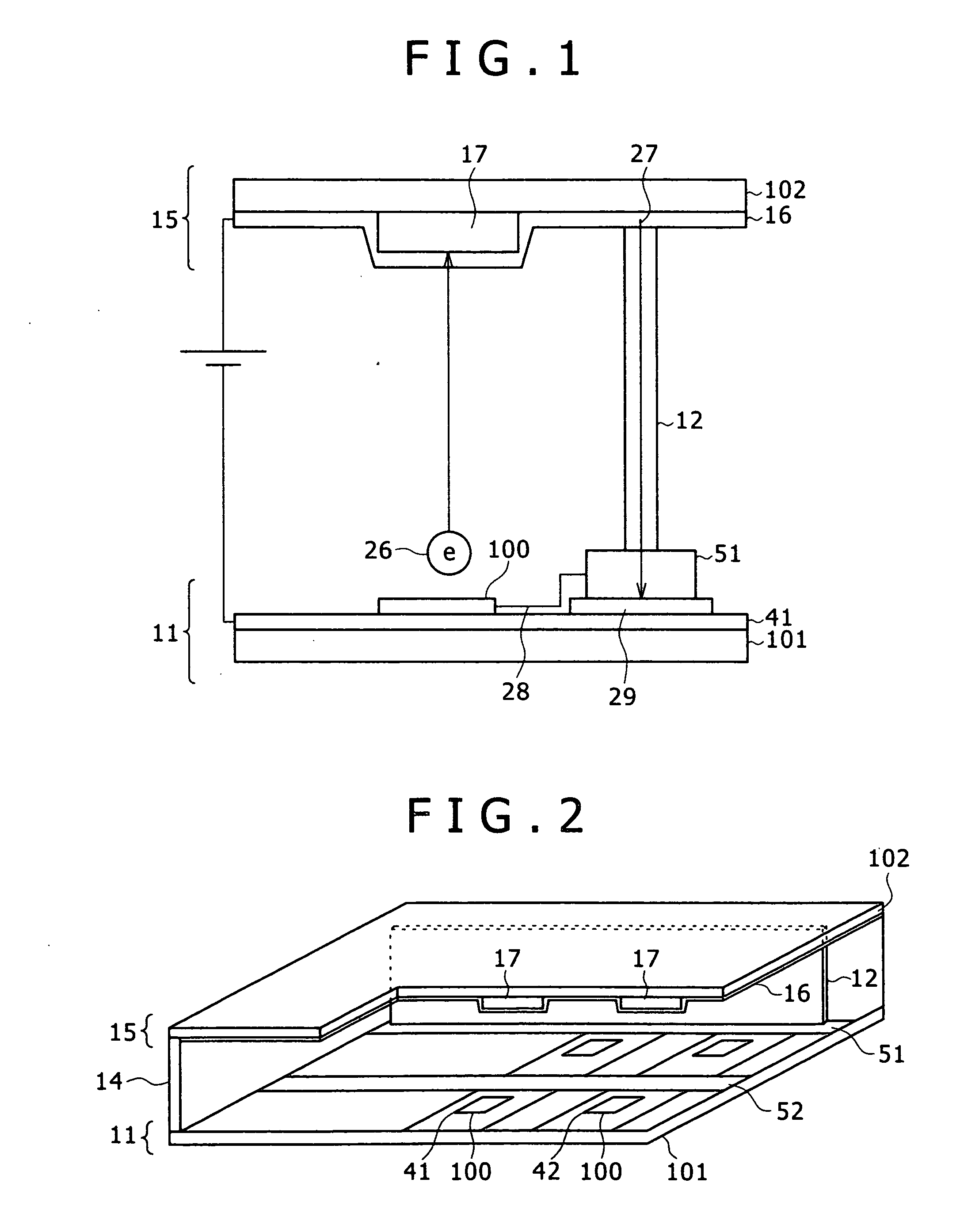
[0035]FIG. 2 is a cross section view of an FED display panel. A structure of the display panel is described using FIG. 2. The display panel includes a cathode substrate 11, an anode substrate 15, and a spacer 12, and flit glass 14.

[0036] A space is formed between the cathode substrate 11 and the anode substrate 15, which is evacuated into a vacuum atmosphere. The circumference of the cathode substrate 11 and the anode substrate 15 is sealed by the flit glass 14 for vacuum lock.

[0037] The spacer 12 is disposed for bearing the atmospheric pressure applied to the disp...

embodiment 2

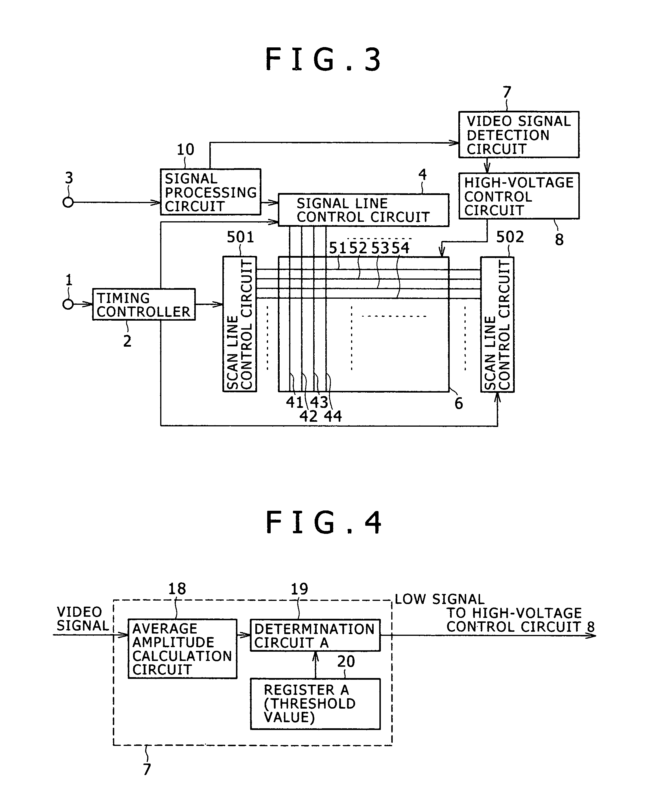
[0057] Next, a second embodiment of the present invention is described using FIG. 3 and FIG. 8.

[0058] The embodiment is approximately the same as the first embodiment, but different from the first embodiment in a configuration of the video signal detection circuit 7. FIG. 8 is a diagram showing the configuration of the video signal detection circuit 7 in the embodiment. The video signal from the signal processing circuit 10 is inputted into a maximum amplitude calculation circuit 21 configuring the video signal detection circuit 7. The maximum amplitude calculation circuit 21 calculates maximum amplitude of the inputted video signal, and outputs a calculation result to a determination circuit B22. The determination circuit B22 compares a threshold value stored in a register B23 to the calculation result, and when the calculation result has a value that is lower than the threshold value, the circuit outputs a signal (Low signal) for performing control of decreasing the high voltage ...

embodiment 3

[0060] Next, a third embodiment of the present invention is described using FIG. 10 and FIG. 11.

[0061]FIG. 10 is a diagram showing a configuration example of a circuit block in the embodiment. FIG. 10 is different from FIG. 3 in that a timing pulse for the video signal is inputted from the timing controller 2 into the video signal detection circuit 7, but is the same as FIG. 3 in other points. In FIG. 10, components marked with the same signs as in FIG. 3 have the same functions.

[0062]FIG. 11 is a diagram showing a configuration of the video signal detection circuit 7 in the embodiment, and FIG. 12 is a timing chart diagram of the high voltage value controlled in the embodiment and a vertical retrace period. The timing pulse for the video signal outputted from the timing controller 2 is inputted into a determination circuit C24 configuring the video signal detection circuit 7. The determination circuit C24 determines the vertical retrace period from the inputted timing pulse, and ...


PUM


Abstract

An image display device according to the present invention has: a cathode plate on which plural electron emission elements for emitting electrons are provided; an anode plate having phosphors and a metal back, the plate being disposed facing the cathode plate; spacers for supporting the cathode plate and the anode plate; a high-voltage control circuit for controlling high voltage between respective two ends of the spacers. In a video signal detection circuit, at least one of features of the inputted video signal, for example, average amplitude, maximum amplitude, a horizontal synchronizing signal, or a vertical synchronizing signal is detected, and when a result of the detection meets a predetermined condition, the high voltage applied to the two ends of the spacers is decreased, thereby the current flowing into the spacers is decreased.

Description

CLAIM OF PRIORITY [0001] The present application claims priority from Japanese application Serial No. JP 2005-159262, filed on May 31, 2005, the content of which is hereby incorporated by reference into this application. BACKGROUND OF THE INVENTION [0002] 1. Field of the Invention [0003] The present invention relates to an image display device such as a field or electron emission display (FED), and in particular, relates to reduction in power consumption during driving FED. [0004] 2. Description of the Related Art [0005]FIG. 1 is a view showing an example of an internal structure of an FED panel. The related art on FED is described using FIG. 1. [0006] The FED has a cathode substrate 11 on which plural electron emission elements 100 are provided, and an anode substrate 15 including phosphors 17, which is disposed facing the cathode substrate. The electron emission elements 100 are bonded to scan lines 51 via connection electrodes 28, and furthermore connected to signal lines 41. Vol...

Claims


Application Information

Patent Timeline
IPC IPC(8): H05B39/00
CPCH05B41/28H05B37/0209H05B47/10
Inventor SATOH, JUNICHIHARUNA, FUMIO
Owner HITACHI LTD
Why Eureka
Try Eureka