
Semiconductor memory apparatus, semiconductor integrated circuit having the same, and method of outputting data in semiconductor memory apparatus

Active Publication Date: 2008-07-17
SK HYNIX INC
View PDF10 Cites 2 Cited by
  • Summary
  • Abstract
  • Description
  • Claims
  • Application Information

AI Technical Summary

Benefits of technology

[0012]Embodiments of the present invention provide a semiconductor memory apparatus that increases a time margin between output data and a data output strobe signal, a semiconductor integrated circuit having the same, and a method of outputting data in a semiconductor memory apparatus.

Problems solved by technology

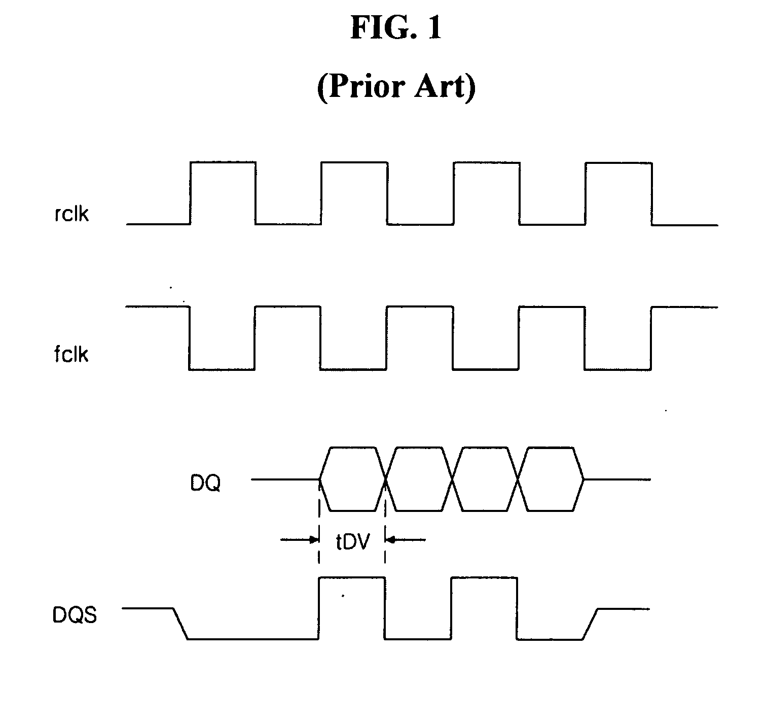
This makes it difficult for the memory control apparatus, which controls the semiconductor memory apparatus, to restore the data.
As described above, in the related art, it is difficult to secure a time margin between the output data and the data output strobe signal according to the increase in execution speed of the semiconductor memory apparatus.

Method used


Image

  • Semiconductor memory apparatus, semiconductor integrated circuit having the same, and method of outputting data in semiconductor memory apparatus
  • Semiconductor memory apparatus, semiconductor integrated circuit having the same, and method of outputting data in semiconductor memory apparatus
  • Semiconductor memory apparatus, semiconductor integrated circuit having the same, and method of outputting data in semiconductor memory apparatus

Examples


Embodiment Construction

[0021]Hereinafter, exemplary embodiments of the present invention will be described in detail with reference to the accompanying drawings.

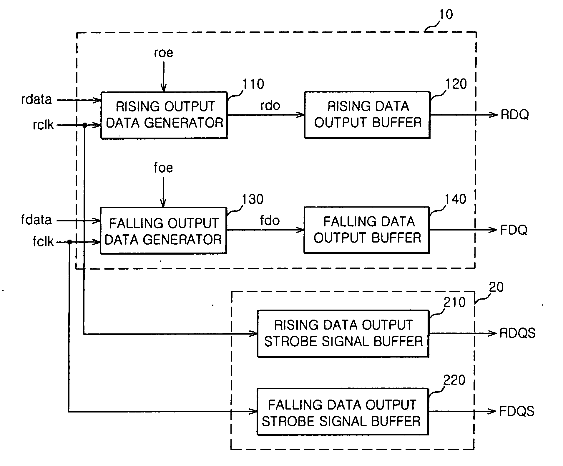
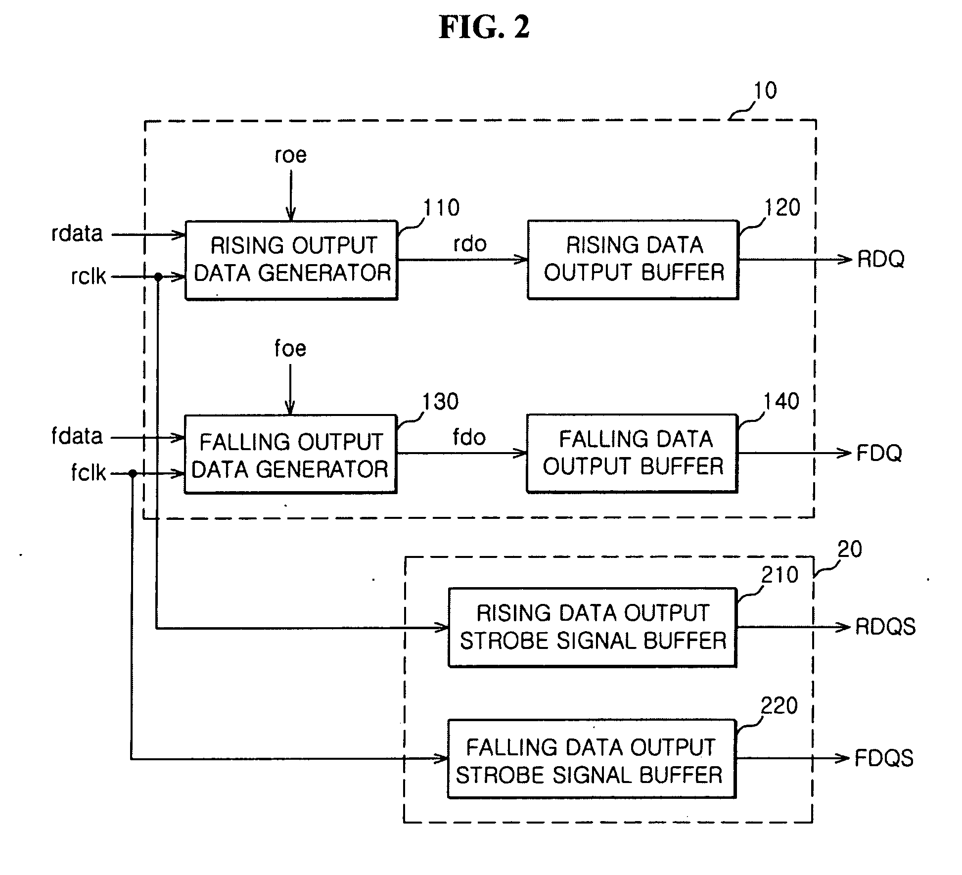
[0022]Referring to FIG. 2, a data output circuit may include a data output unit 10 and a data output strobe signal generation unit 20.

[0023]The data output unit 10 may include a rising output data generator 110, a rising data output buffer 120, a falling output data generator 130, and a falling data output buffer 140.

[0024]The rising output data generator 110 generates rising output data rdo using rising data rdata in response to a rising clock rclk and a rising output enable signal roe.

[0025]The rising data output buffer 120 buffers the rising output data rdo, thereby outputting final rising output data RDQ.

[0026]The falling output data generator 130 generates falling output data fdo using falling data fdata in response to a falling clock fclk and a falling output enable signal foe.

[0027]The falling data output buffer 140 buffers the falling outp...


PUM


Abstract

A semiconductor memory apparatus includes a rising output data generator that generates rising output data from rising data in response to a rising clock and a rising output enable signal. A rising data output buffer buffers the rising output data. A falling output data generator generates falling output data from falling data in response to a falling clock and a falling output enable signal. A falling data output buffer buffers the falling output data.

Description

CROSS-REFERENCE TO RELATED PATENT APPLICATION[0001]This application claims the benefit of Korean Patent Application No. 10-2007-0003646, filed on Jan. 12, 2007, in the Korean Intellectual Property Office, the disclosure of which is incorporated herein in its entirety by reference.BACKGROUND OF THE INVENTION[0002]1. Technical Field[0003]The present invention relates to a semiconductor memory apparatus, a semiconductor integrated circuit having the same, and a method of outputting data in a semiconductor memory apparatus. In particular, the present invention relates to a semiconductor memory apparatus that increases a time margin between output data and a data output strobe signal, a semiconductor integrated circuit having the same, and a method of outputting data in a semiconductor memory apparatus.[0004]2. Related Art[0005]Generally, in a DDR SDRAM (Double Data Rate Synchronous Dynamic Random Access Memory) and a semiconductor memory apparatus more advanced than the DDR SDRAM, data ...

Claims


Application Information

Patent Timeline
IPC IPC(8): G11C8/00
CPCG11C7/1051G11C7/1057G11C7/1066G11C11/4093G11C7/22G11C7/225G11C11/4076G11C7/1072G11C7/10G11C11/407
Inventor KU, KIE BONG
Owner SK HYNIX INC
Learn More