Nonvolatile semiconductor memory and process of producing the same

a semiconductor memory and non-volatile technology, applied in semiconductor devices, transistors, instruments, etc., can solve the problems of difficult removal of charge storage layers, difficult control of threshold voltage, and limit to the reduction of processing measurements and physical dimensions of memory cells

Active Publication Date: 2008-07-24
KIOXIA CORP
View PDF13 Cites 315 Cited by
  • Summary
  • Abstract
  • Description
  • Claims
  • Application Information

AI Technical Summary

Benefits of technology

[0012]A nonvolatile semiconductor memory of an aspect of the present invention comprises: a semiconductor substrate; a pillar-shaped semiconductor layer extending in a vertical direction with respect to a surface of the semiconductor substrate; a plurality of memory cells arranged in the vertical direction on a side surface of the semiconductor layer and having a charge storage layer and a control gate electrode; a first select gate transistor arranged on the semiconductor subs

Problems solved by technology

There is a limit, however, to reduction of processing measurements and physical dimensions of the memory cells because these factors depend on the manufacturing equipment.
On the other hand, for a select gate transistor on the bottom end of the memory cell, or in other words, on the semiconductor substrate side, a charge storage layer is very difficult to remove

Method used


Image

  • Nonvolatile semiconductor memory and process of producing the same
  • Nonvolatile semiconductor memory and process of producing the same
  • Nonvolatile semiconductor memory and process of producing the same

Examples


Embodiment Construction

[0037]Embodiments of the present invention will be explained in detail below with reference to the attached drawings.

1. Overview

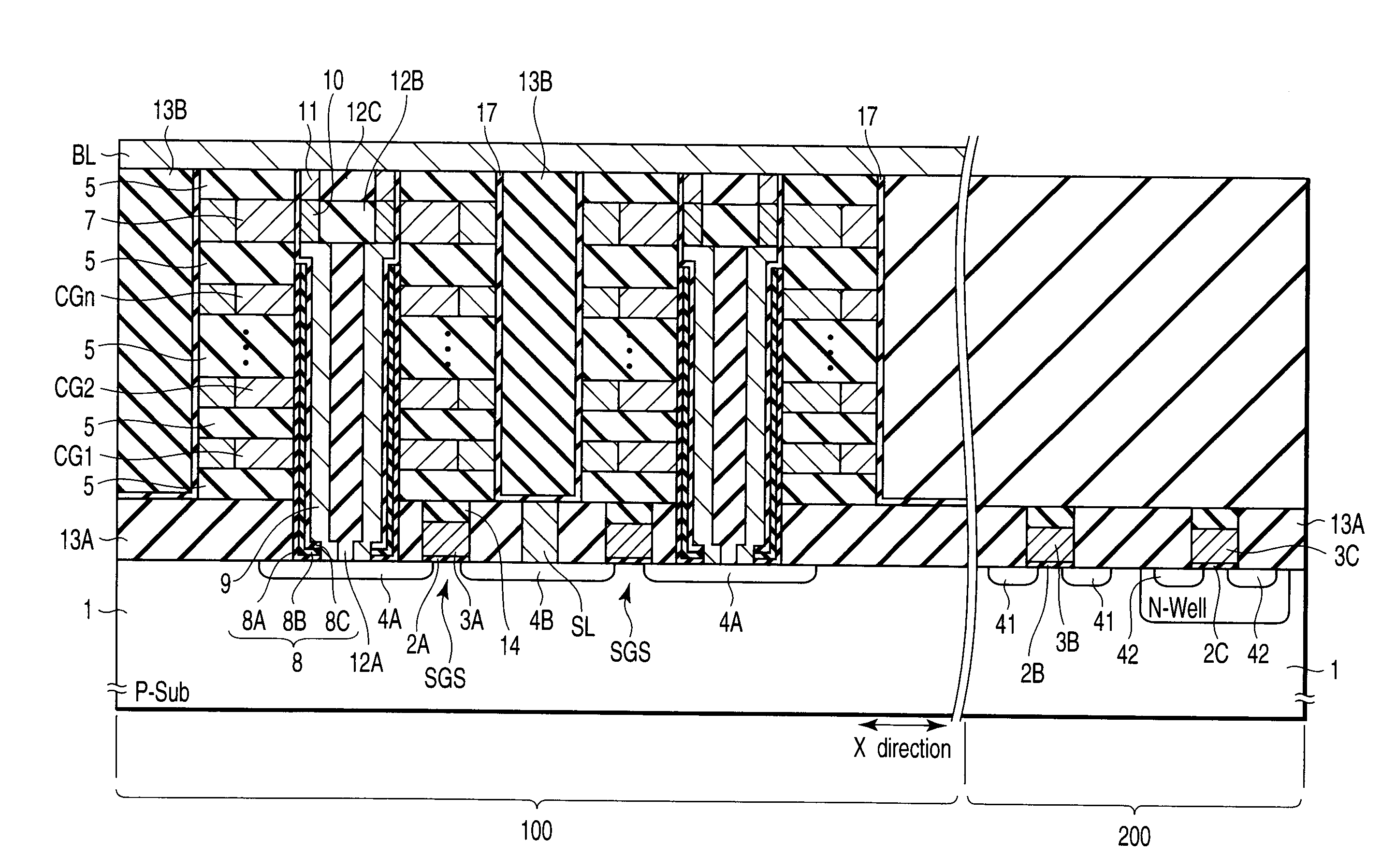
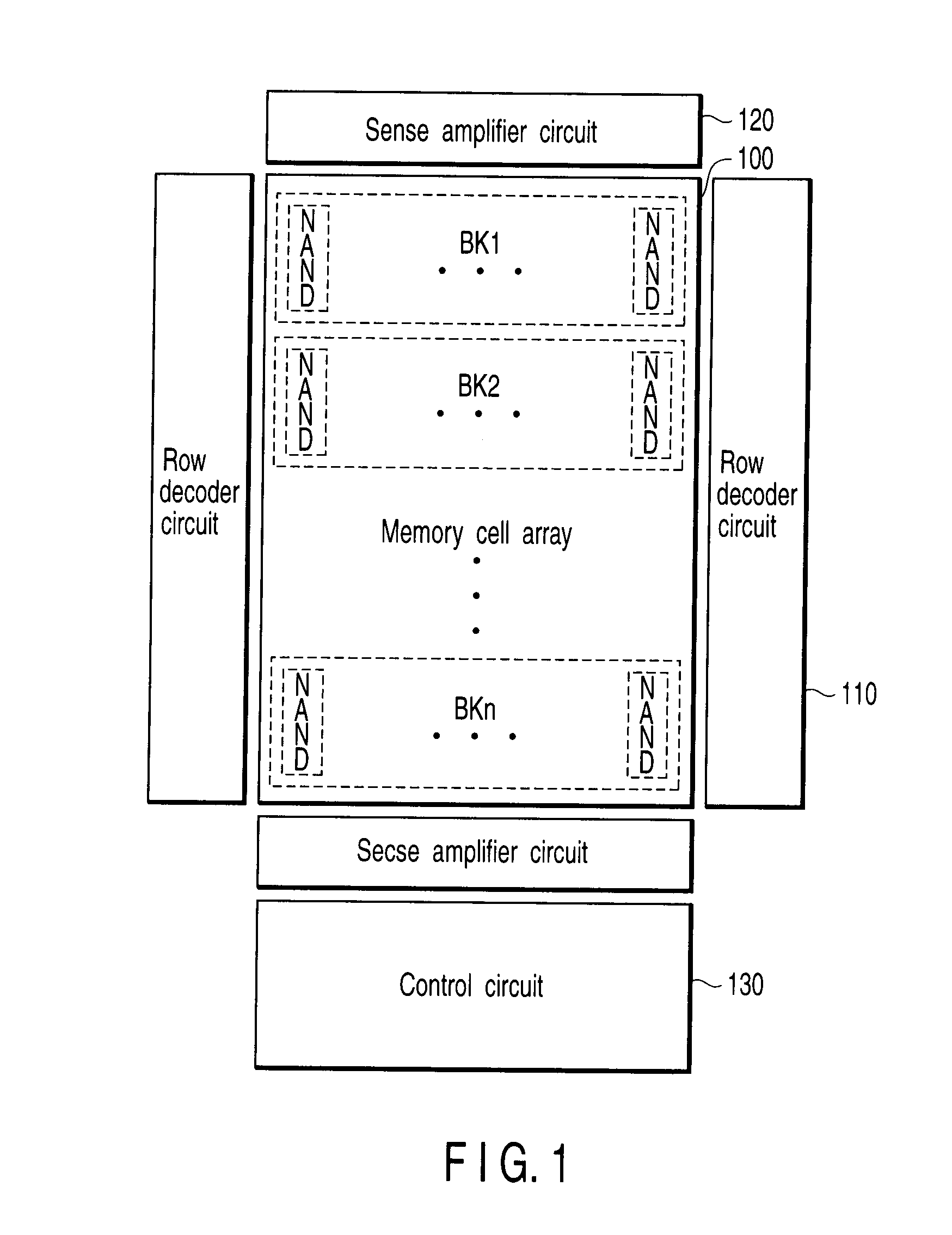
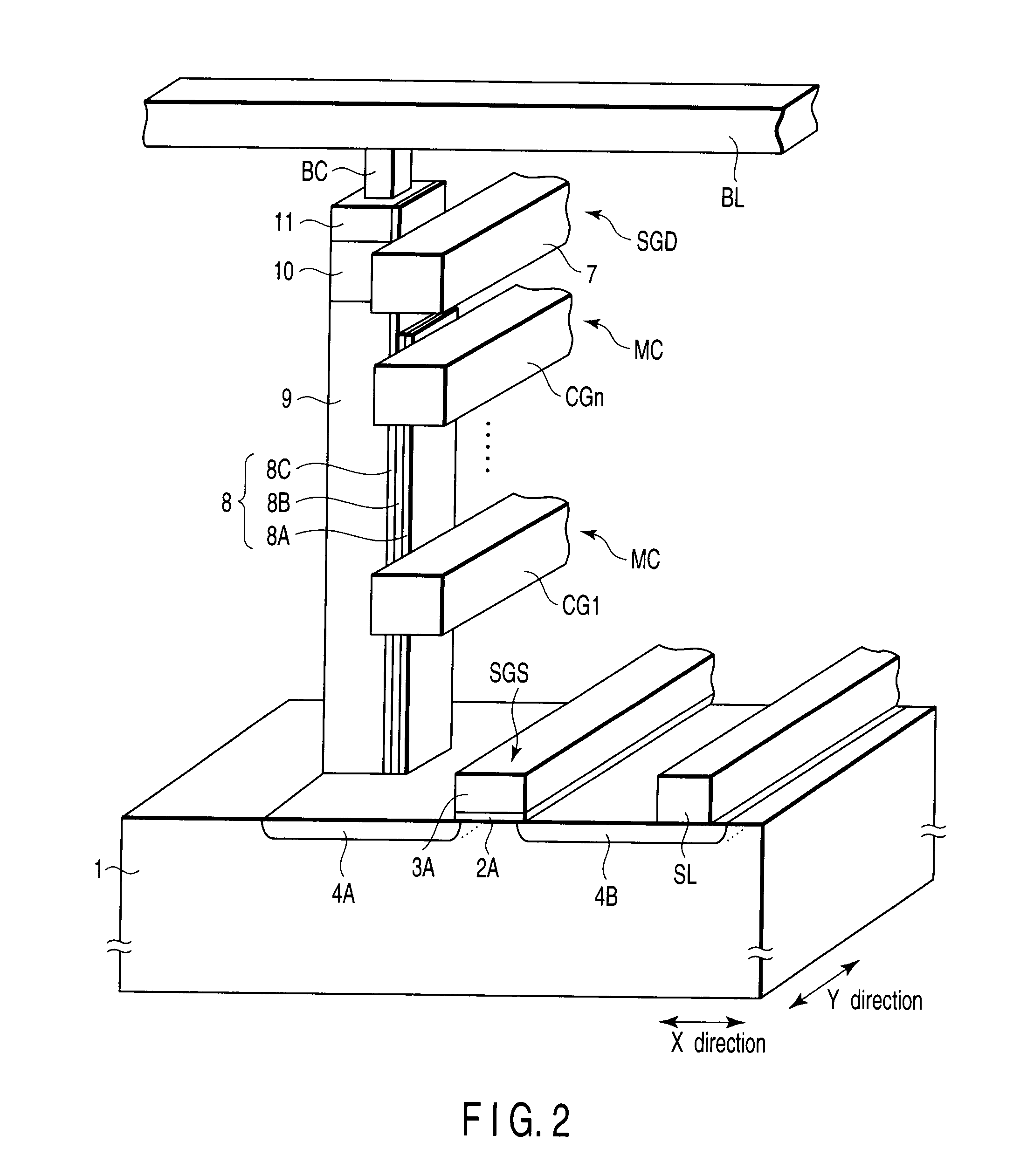
[0038]A nonvolatile semiconductor memory according to an aspect of the present invention includes multiple vertical memory cell transistors arranged along a side surface of a pillar-shaped semiconductor layer extending in a vertical direction with respect to the surface of the semiconductor substrate. The source / drain regions of the vertical memory cell transistors are arranged in the semiconductor layer. The source / drain regions of one memory cell transistor are shared with other memory cell transistors so that the memory cell transistors are connected to one another in series. A group of memory cell transistors connected in series form a memory cell string. Select gate transistors are arranged on the two sides of the memory cell string, and one of the select gate transistors arranged on the lower end of the memory cell string (on the semiconductor substra...


PUM


Abstract

A nonvolatile semiconductor memory of an aspect of the present invention comprises a semiconductor substrate, a pillar-shaped semiconductor layer extending in the vertical direction with respect to the surface of the semiconductor substrate, a plurality of memory cells arranged in the vertical direction on the side surface of the semiconductor layer and having a charge storage layer and a control gate electrode, a first select gate transistor arranged on the semiconductor layer at an end of the memory cells on the side of the semiconductor substrate, and a second select gate transistor arranged on the semiconductor layer on the other end of the memory cells opposite to the side of the semiconductor substrate, wherein the first select gate transistor includes a diffusion layer in the semiconductor substrate and is electrically connected to the pillar-shaped semiconductor layer by way of the diffusion layer that serves as the drain region.

Description

CROSS-REFERENCE TO RELATED APPLICATIONS[0001]This application is based upon and claims the benefit of priority from prior Japanese Patent Application No. 2006-344803, filed Dec. 21, 2006, the entire contents of which are incorporated herein by reference.BACKGROUND OF THE INVENTION[0002]1. Field of the Invention[0003]The present invention relates to a nonvolatile semiconductor memory, especially to a flash memory using memory cells in each of which a charge storage layer and a gate electrode are stacked together.[0004]2. Description of the Related Art[0005]A nonvolatile semiconductor memory such as a NAND-type semiconductor memory has been employed as a memory device for various kinds of electronic equipment.[0006]Recently, memory cells are more finely designed than ever in order to increase their memory capacities and integration densities. There is a limit, however, to reduction of processing measurements and physical dimensions of the memory cells because these factors depend on t...

Claims


Application Information

Patent Timeline
IPC IPC(8): H01L29/00H01L21/336
CPCG11C16/0483H01L27/11524H01L29/7926H01L27/11556H01L29/792H01L27/11529H10B41/41H10B41/35H10B41/27H10B63/30
Inventor ARAI, FUMITAKASHIROTA, RIICHIRO
Owner KIOXIA CORP
Why Eureka
Try Eureka