Memory cell of a resistive semiconductor memory device, a resistive semiconductor memory device having a three-dimensional stack structure, and related methods

a memory cell and semiconductor technology, applied in the direction of information storage, static storage, digital storage, etc., can solve the problems of high operation speed, low power consumption, and the degree of integration of a semiconductor memory device having a two-dimensional structure is approaching an upper limit, so as to improve reliability and high degree of integration

Active Publication Date: 2008-07-24
SAMSUNG ELECTRONICS CO LTD
View PDF10 Cites 121 Cited by
  • Summary
  • Abstract
  • Description
  • Claims
  • Application Information

AI Technical Summary

Benefits of technology

[0020]Embodiments of the invention provide a memory cell of a resistive semiconductor memory device, a resistive semiconductor memory device having a three-dimensional stack structure, and a method for controlling the resistive semiconductor memory device. The resistive semiconductor memory device, in accordance with an embodiment of the invention, may have a relatively high degree of integration, and may sense a data value stored in a memory cell more reliably than a conventional device and therefore may have improved reliability.

Problems solved by technology

Therefore, it is expected that demand for semiconductor memory devices using diode structures as memory cells and having relatively high integration densities, relatively high operation speeds, relatively low power consumption will increase.
However, the degree of integration of a semiconductor memory device having a two-dimensional structure is approaching an upper limit.
Further, since memory cells of the resistive memory device described above have various resistance distributions, a sensing margin for accurately sensing the data value “0” and the data value “1” cannot be sufficiently guaranteed.

Method used


Image

  • Memory cell of a resistive semiconductor memory device, a resistive semiconductor memory device having a three-dimensional stack structure, and related methods
  • Memory cell of a resistive semiconductor memory device, a resistive semiconductor memory device having a three-dimensional stack structure, and related methods
  • Memory cell of a resistive semiconductor memory device, a resistive semiconductor memory device having a three-dimensional stack structure, and related methods

Examples


Embodiment Construction

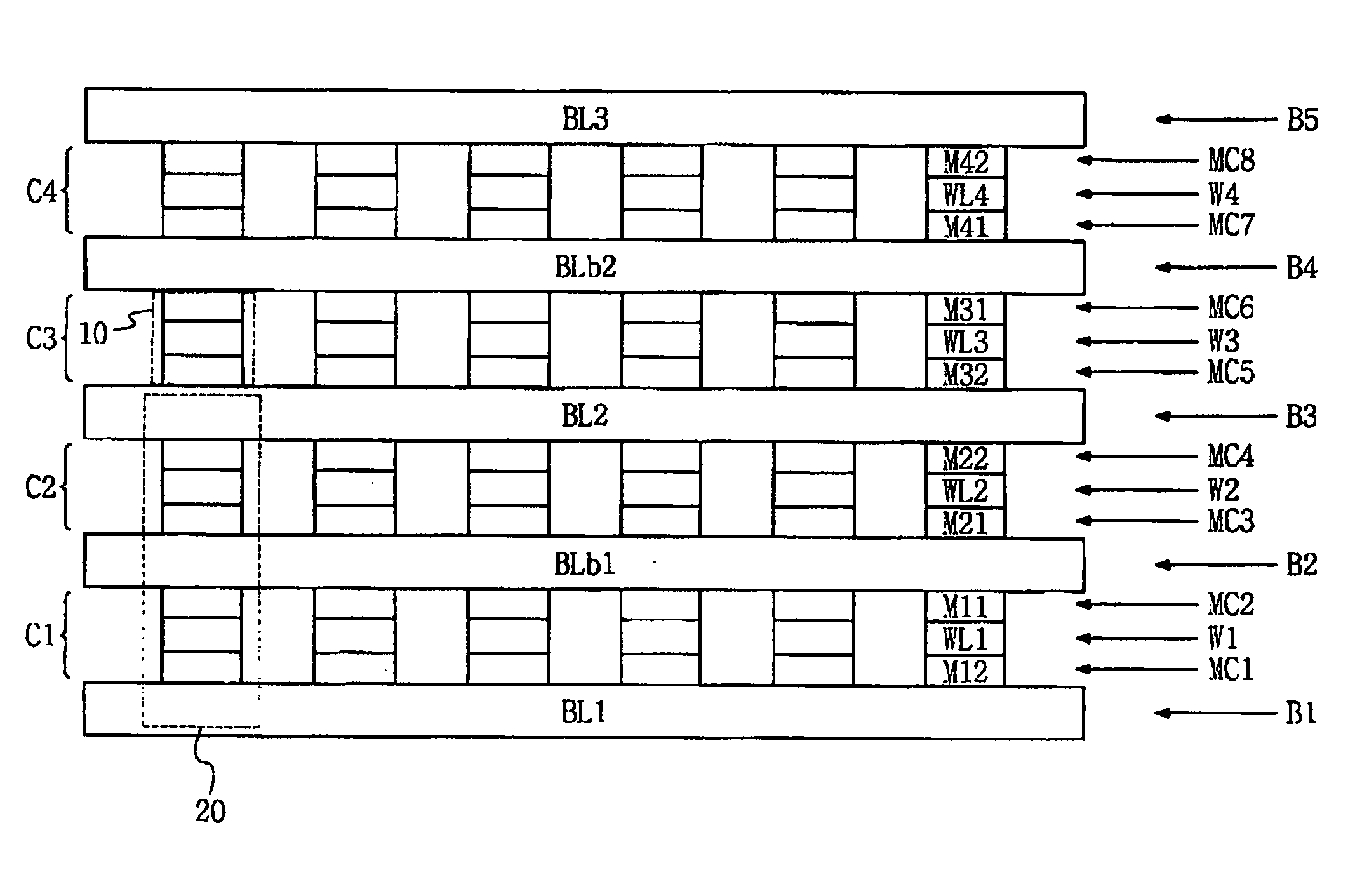
[0040]In the drawings, like reference symbols indicate like or similar components throughout.

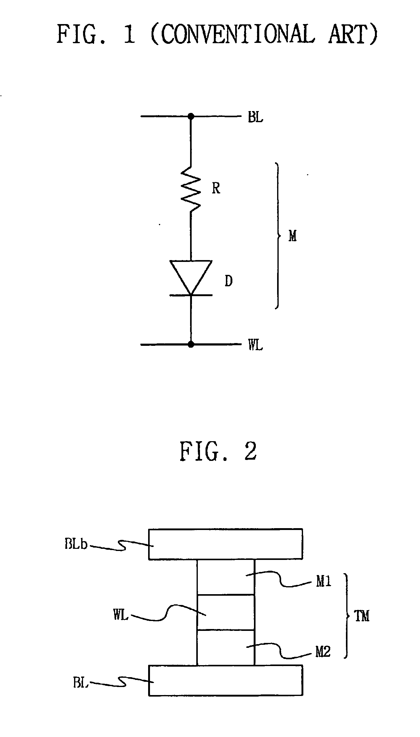
[0041]FIG. 2 illustrates the structure of a memory cell of a resistive semiconductor memory device in accordance with an embodiment of the invention.

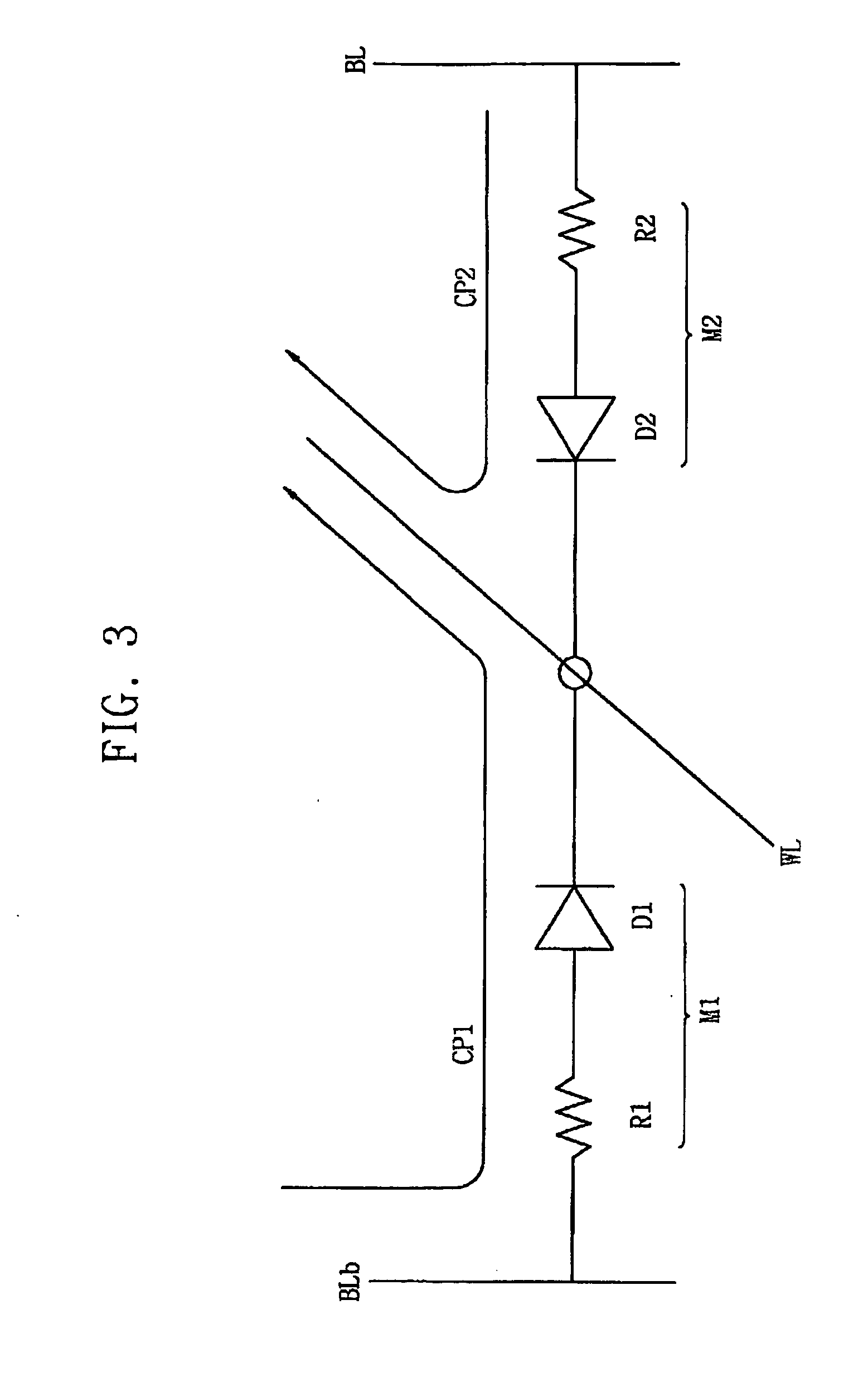
[0042]As shown in FIG. 2, a memory cell TM in accordance with an embodiment of the invention has a twin cell structure. Thus, memory cell TM can store one more bit of data than a conventional memory cell (e.g., conventional memory cell M of FIG. 1). Memory cell TM comprises a main unit cell M2 connected to a main bit line BL and a sub unit cell M1 connected to a sub bit line BLb. In addition, main unit cell M2 and sub unit cell M1 are each connected to a word line WL (that is, they are each connected to the same word line WL). While the conventional memory cell M described above (with reference to FIG. 1) has one diode D and one variable resistor R, memory cell TM in accordance with an embodiment of the invention has a structure in which main un...


PUM


Abstract

A memory cell of a resistive semiconductor memory device, a resistive semiconductor memory device having a three-dimensional stack structure, and related methods are provided. The memory cell of a resistive semiconductor memory device includes a twin cell, wherein the twin cell stores data values representing one bit of data. The twin cell includes a main unit cell connected to a main bit line and a word line, and a sub unit cell connected to a sub bit line and the word line. Also, the main unit cell includes a first variable resistor and a first diode, and the sub unit cell includes a second variable resistor and a second diode.

Description

CROSS-REFERENCE TO RELATED APPLICATION[0001]This application claims priority to Korean Patent Application No. 10-2007-0006859, filed Jan. 23, 2007, the subject matter of which is hereby incorporated by reference in its entirety.BACKGROUND OF THE INVENTION[0002]1. Field of the Invention[0003]Embodiments of the invention relate to a semiconductor memory device, a memory cell of a semiconductor memory device, and a method for controlling the device. In particular, embodiments of the invention relate to a resistive semiconductor memory device having a three-dimensional stack structure, a memory cell of the resistive semiconductor memory device, and a method for controlling the device.[0004]2. Description of Related Art[0005]Because of the need for memory devices having relatively high storage capacity and relatively low power consumption, memory devices that are non-volatile and do not require refreshing are being studied. These memory devices, which are presently considered to be “next...

Claims


Application Information

Patent Timeline
Patent Type & Authority Applications(United States)
IPC IPC(8): G11C5/02G11C11/21
CPCG11C5/02G11C13/00G11C2213/72G11C13/0023G11C2213/71G11C13/0004G11C7/18
Inventor PARK, JOON-MINKANG, SANG-BEOMOH, HYUNG-ROKCHO, WOO-YEONG
Owner SAMSUNG ELECTRONICS CO LTD
Why Eureka
Try Eureka