Solid-state imaging device and imaging device

a technology of solid-state imaging and imaging device, which is applied in the direction of color signal processing circuit, color television details, television system, etc., can solve the problems of various problems and problems, and achieve the effect of preventing signal level variations and small negative influen

Inactive Publication Date: 2008-07-31
SONY CORP
View PDF1 Cites 79 Cited by
  • Summary
  • Abstract
  • Description
  • Claims
  • Application Information

AI Technical Summary

Benefits of technology

[0052]According to one embodiment of the present invention, relating to the unit pixel to be thinned when in the thinning reading mode, the transfer control potential supplied to the transfer unit is set as a blooming reduction potential so that the charge overflowing at the detecting unit transitions to a state readily transferable to the pixel signal generating unit side. Thus, the unneeded charge which overflowed within the detecting unit transitions to a state readily dischargeable on the pixel signal generating unit side, whereby blooming phenomenon, wherein charge generated at the thinned unit pixels overflows and leaks into the unit pixels of adjacent reading operations, can be suppressed.
[0053]With consideration for the point that the pixel array unit is made up of unit pixel groups with a pixel-sharing configuration, when th...

Problems solved by technology

However, if thinning reading is performed in increments of rows or increments of columns (hereafter this will be written as increments of rows, representatively), driving conditions as to the pixels (driving frequency of transistors) differ between a thinning row wherein a reading operation is not performed and a reading row wherein thinning is not performed, whereby various problems can occ...

Method used


Image

  • Solid-state imaging device and imaging device
  • Solid-state imaging device and imaging device
  • Solid-state imaging device and imaging device

Examples


Embodiment Construction

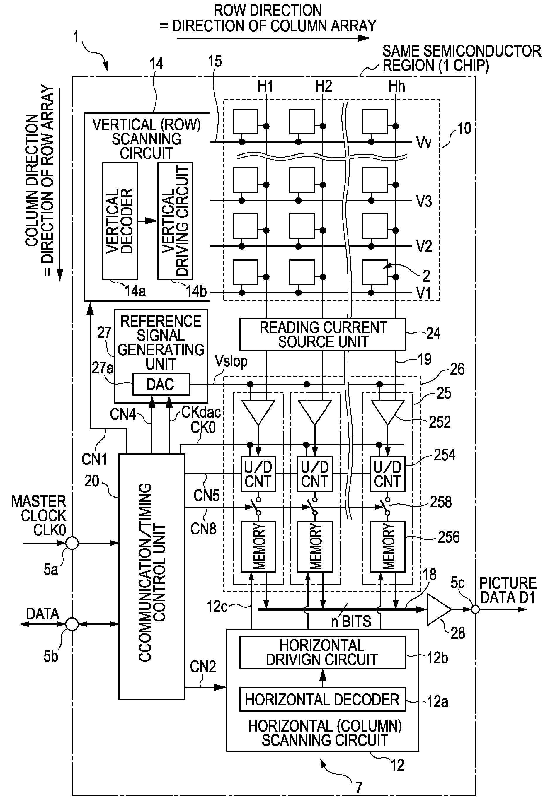
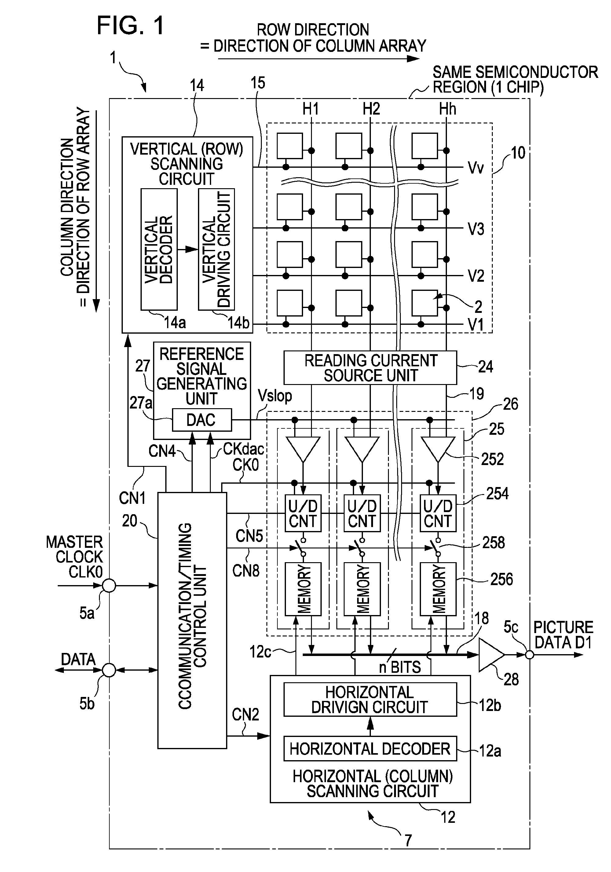
[0078]Embodiments according to the present invention will be described in detail below with reference to the diagrams. Note that an example will be described below wherein a CMOS solid-state imaging device, which is an example of a solid-state imaging device of an X-Y address form, is used as a device. Also, the CMOS solid-state imaging device is described as all pixels being formed from NMOS.

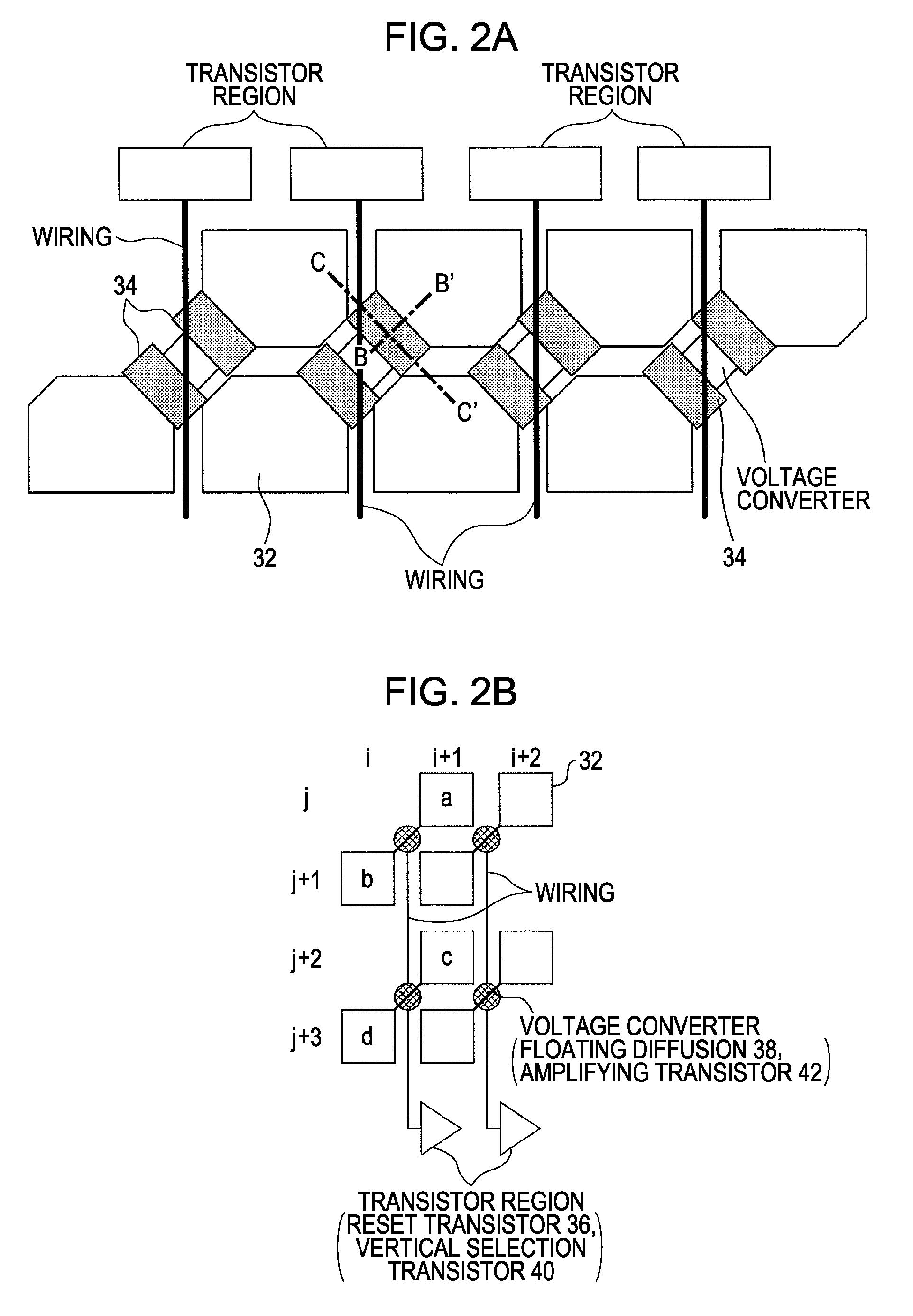
[0079]In particular, with the solid-state imaging device of the present embodiment, unit configuration elements making up a pixel array unit have a feature of having a unit pixel group of a pixel sharing configuration with a configuration, wherein a portion of the elements within the unit pixels are shared with multiple unit pixels.

[0080]However, this is only one example, and the object device is not limited to a MOS-type solid-state imaging device. All of the embodiments to be described later can be similarly applied to all semiconductor devices for physical quantity distribution detecting, wh...


PUM


Abstract

A solid-state imaging device includes: a pixel array unit wherein a unit pixel group with a portion of elements of a unit pixel being shared with a plurality of unit pixels is arrayed in a matrix form, the unit pixel having a detecting unit, a pixel signal generating unit, a transfer unit to transfer the charge, and an initializing unit to initialize the potential of the pixel signal generating unit; and a driving control unit; wherein the driving control unit controls blooming reduction potential which is the transfer control potential supplied to the transfer unit of the unit pixel to be thinned, so that the overflow charge at the detecting unit with the unit pixel to be thinned which has no shared relation with the unit pixel to be read transitions to a state readily transferable to the pixel signal generating unit side of the unit pixel to be thinned.

Description

CROSS REFERENCES TO RELATED APPLICATIONS[0001]The present invention contains subject matter related to Japanese Patent Application JP 2007-004755 and Japanese Patent Application JP 2007-004756, both filed in the Japanese Patent Office on Jan. 12, 2007, the entire contents of which are incorporated herein by reference.BACKGROUND OF THE INVENTION[0002]1. Field of the Invention[0003]The present invention relates to a solid-state imaging device and an imaging device which are examples of a semiconductor device for physical quantity distribution detection. Specifically, the present invention relates to an arrangement wherein multiple unit configuration elements are arrayed which has sensitivity as to an electromagnetic wave input externally such as light or a radiation beam for example, and reads the physical quantity distribution converted to an electrical signal by the unit configuration elements as an analog electrical signal or digital data. Particularly, the present invention relate...

Claims


Application Information

Patent Timeline
IPC IPC(8): H04N5/217H04N5/345H04N5/357H04N5/3745
CPCH04N5/3452H04N5/37455H04N5/37452H04N5/3594H04N25/441H04N25/623H04N25/772H04N25/771
Inventor SATO, MAKISUZUKI, RYOJIFUJITA, NORITAKAKAMOGAWA, SATSUKI
Owner SONY CORP
Why Eureka
Try Eureka