Electronic package structure

a technology of electronic package and electronic components, applied in the field can solve the problems of unsatisfactory heat dissipation capacity of electronic package structure b>200/b>, very high fabrication and high cost of electronic package structure b>100/b>, and achieve the effect of high efficiency of utilizing internal spa

Inactive Publication Date: 2008-07-31
CYNTEC
View PDF33 Cites 24 Cited by
  • Summary
  • Abstract
  • Description
  • Claims
  • Application Information

AI Technical Summary

Benefits of technology

[0010]Accordingly, the present invention is directed to an electronic p...

Problems solved by technology

Electronic package structures are fabricated through very complicated package processes.
Besides, the fabricating cost of the electronic package structure 100 is very high for these...

Method used


Image

  • Electronic package structure
  • Electronic package structure
  • Electronic package structure

Examples


first embodiment

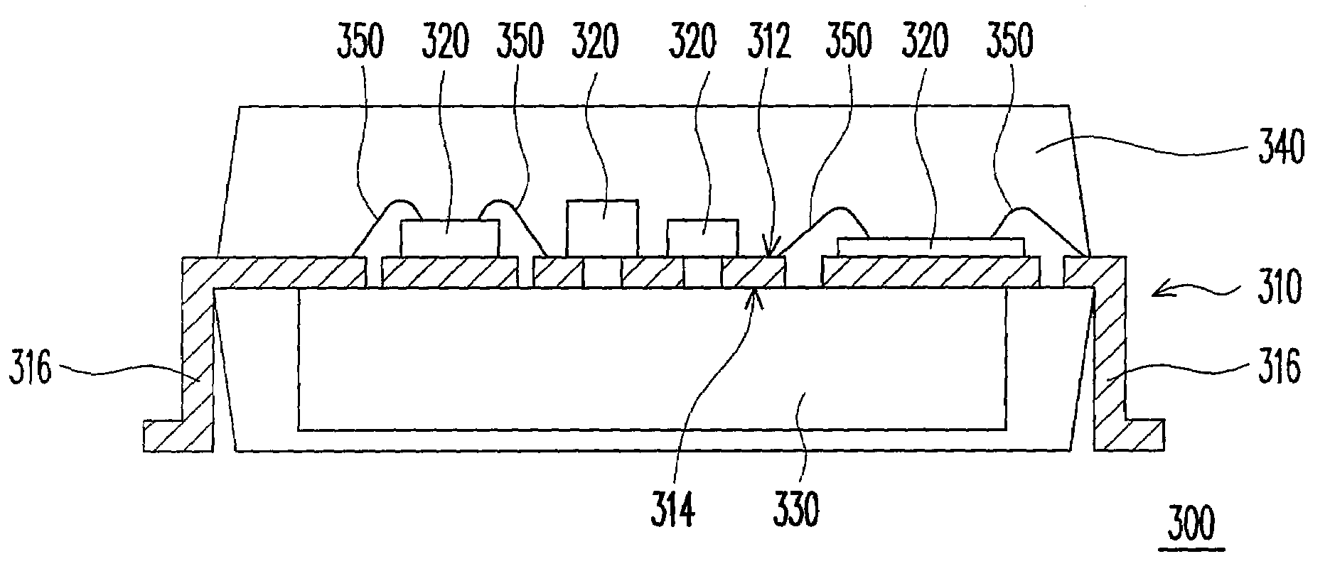
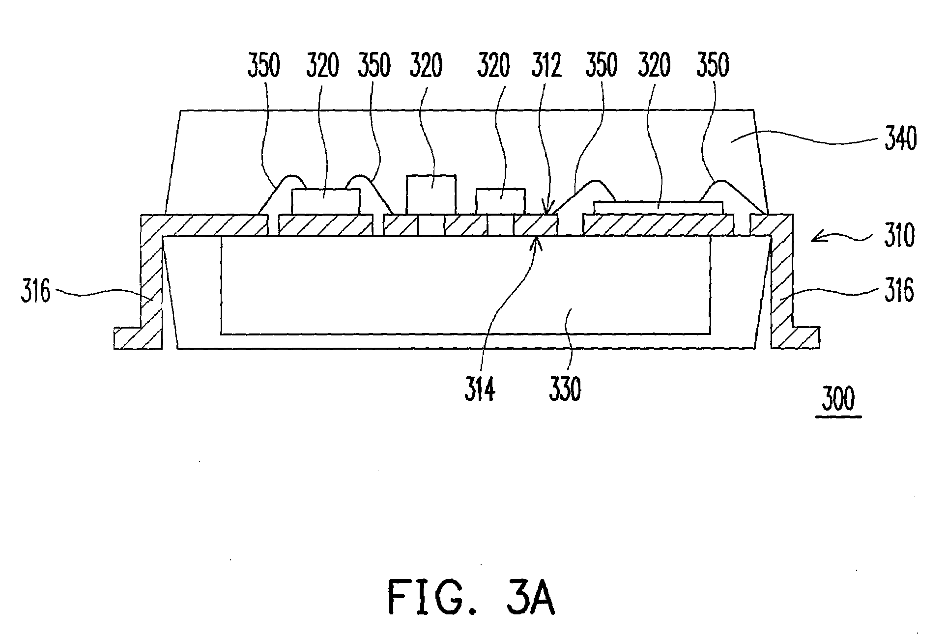
[0027]FIG. 3A is a schematic side view of an electronic package structure according to the first embodiment of the present invention. Referring to FIG. 3A, the electronic package structure 300 includes a first carrier 310 (for example, a leadframe), at least one first electronic element 320 (4 first electronic elements 320 are demonstratively illustrated in FIG. 3), and a second electronic element 330. The first carrier 310 has a first carrying surface 312 and a second carrying surface 314 opposite to each other. The first electronic elements 320 are disposed above the first carrying surface 312 and electrically connected to the first carrier 310. The second electronic element 330 is disposed on the second carrying surface 314 and electrically connected to the first carrier 310. The volume of the second electronic element 330 is greater than that of the first electronic element 320.

[0028]Since the second electronic element 330 having larger volume can be disposed on the second carry...

second embodiment

[0035]FIG. 4 is a schematic side view of an electronic package structure according to a second embodiment of the present invention. Referring to FIG. 4, the main difference of the electronic package structure 400 in the present embodiment from the electronic package structures 300 and 300′ in the first embodiment is that the electronic package structure 400 further includes a second carrier 460. Some of the first electronic elements 420 are disposed on the second carrier 460 and electrically connected to the second carrier 460. The second carrier 460 is disposed on the first carrying surface 412 of the first carrier 410 and electrically connected to the first carrier 410. The second carrier 460 may be a wiring board.

[0036]The second carrier 460, which may be a wiring board, is composed of a plurality of wiring layers (not shown) and a plurality of dielectric layers (not shown) which are stacked together alternatively At least two of the wiring layers are electrically connected to ea...


PUM


Abstract

An electronic package structure including a first carrier, at least one first electronic element, and a second electronic element is provided. The first carrier has a first carrying surface and a second carrying surface opposite to each other. The first electronic element is disposed above the first carrying surface and electrically connected to the first carrier. The second electronic element is disposed on the second carrying surface and electrically connected to the first carrier. The volume of the second electronic element is larger than that of the first electronic element.

Description

CROSS-REFERENCE TO RELATED APPLICATION[0001]This application claims the priority benefit of Taiwan application serial no. 96103493, filed Jan. 31, 2007. All disclosure of the Taiwan application is incorporated herein by reference.BACKGROUND OF THE INVENTION[0002]1. Field of the Invention[0003]The present invention relates to a package structure. More particularly, the present invention relates to an electronic package structure.[0004]2. Description of Related Art[0005]Electronic package structures are fabricated through very complicated package processes. The electronic package structures have different electrical performances and heat dissipation capacities. Thus, a designer may select an electronic package structure having suitable electrical performance and heat dissipation capacity according to his / her own requirement.[0006]FIG. 1 is a schematic diagram of a conventional electronic package structure. Referring to FIG. 1, the conventional electronic package structure 100 includes...

Claims


Application Information

Patent Timeline
IPC IPC(8): H05K7/00
CPCH01L23/495H01L23/49575H01L25/162H01L2224/48091H01L2224/48247H01L2924/19041H01L2924/13055H01L2924/19106H01L2924/30107H01L2924/19105H01L2924/1305H01L24/48H01L2924/13091H01L2924/00014H01L2924/00H01L2224/16245H01L2924/181H01L2924/00012H01L2224/45099H01L2224/45015H01L2924/207
Inventor CHEN, DA-JUNGFANG, CHUNG-SHIUNLU, BAU-RULIN, YI-CHENGWEN, CHAU-CHUN
Owner CYNTEC
Why Eureka
Try Eureka