Solid-state imaging device and imaging apparatus

a technology of imaging device and imaging apparatus, which is applied in the direction of radio frequency controlled devices, instruments, television systems, etc., can solve the problems of affecting image contrast, inability to accurately detect images, and often occur problems, so as to achieve accurate detection and obtain favorable contrast

a technology of imaging device and imaging apparatus, which is applied in the direction of radio frequency controlled devices, instruments, television systems, etc., can solve the problems of affecting image contrast, inability to accurately detect images, and often occur problems, so as to achieve accurate detection and obtain favorable contrast

US20080197268A1Active Publication Date: 2008-08-21SONY SEMICON SOLUTIONS CORP

Image

  • Solid-state imaging device and imaging apparatus
  • Solid-state imaging device and imaging apparatus
  • Solid-state imaging device and imaging apparatus

Examples


Embodiment Construction

[0033]A solid-state imaging device and imaging apparatus according to embodiments of the present invention will be described below with reference to the drawings.

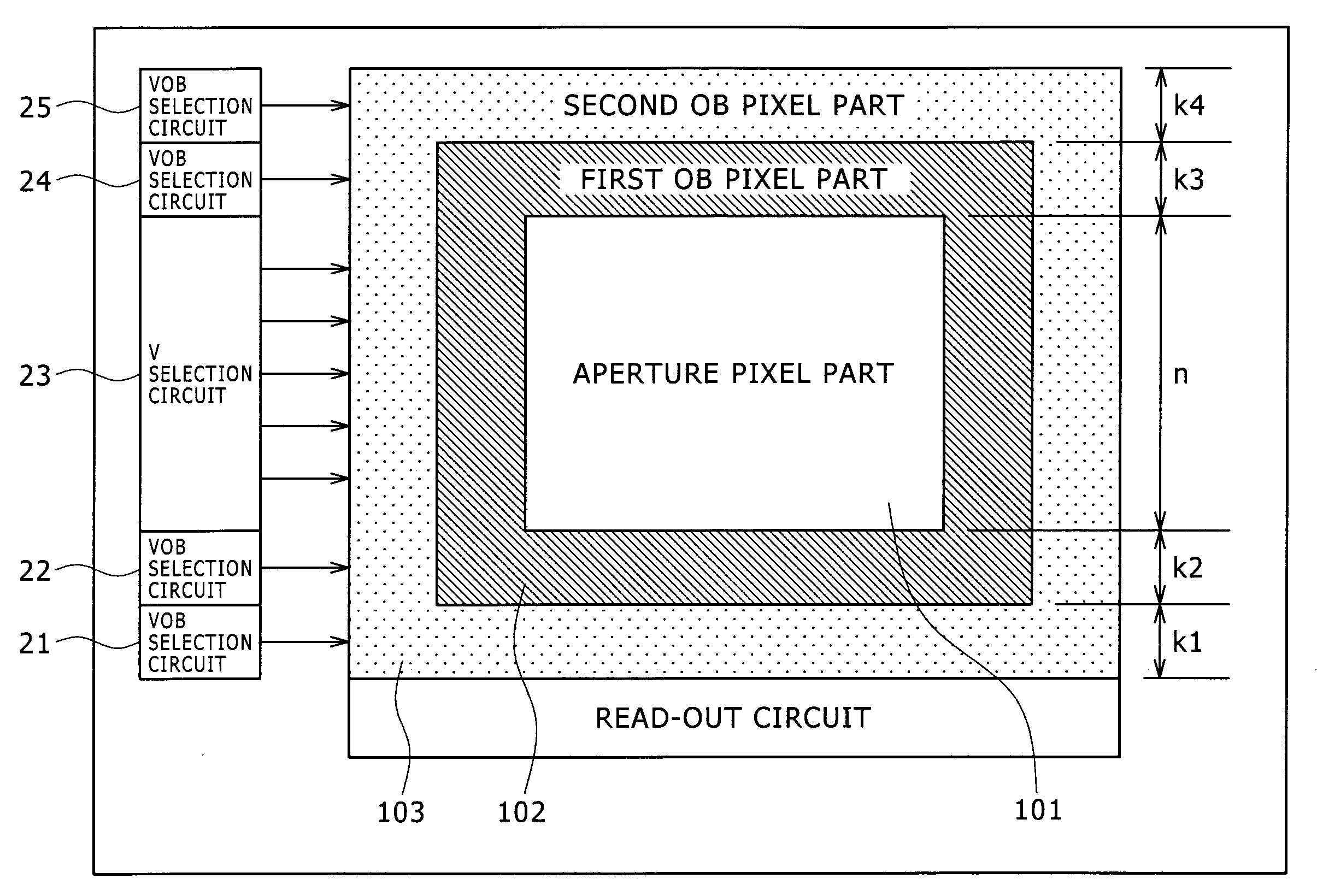
[0034]FIG. 1 is a diagram showing the schematic configuration of the solid-state imaging device according to one embodiment of the present invention.

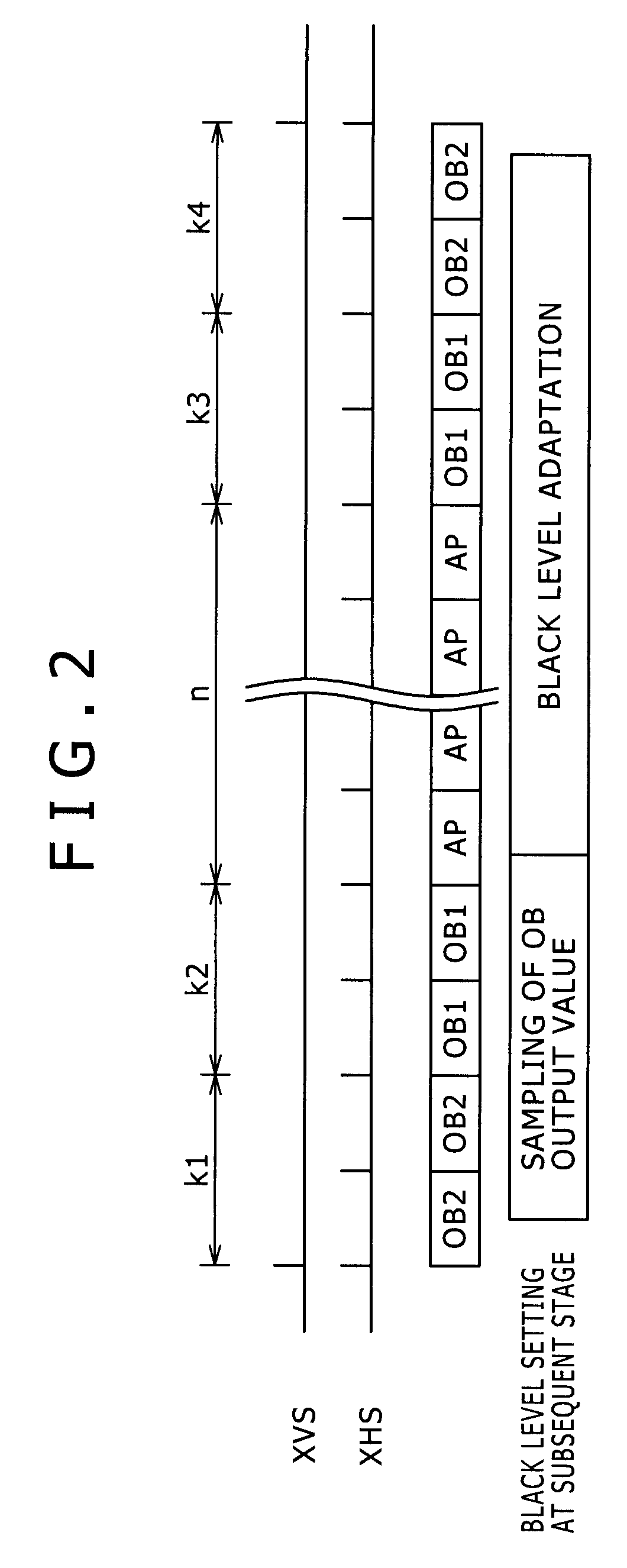
[0035]This solid-state imaging device includes an aperture pixel part 101, a first optical black part 102 provided around the aperture pixel part 101, and a second optical black part 103 provided around the first optical black part 102.

[0036]The aperture pixel part 101 is formed of plural aperture pixels 11 on n rows and plural columns for capturing an image. The first optical black part 102 is formed of plural first OB light-shielded pixels 12 that are shielded from light for detection of an optical black level. The temperature dependence of the dark current in the first OB pixels 12 is larger than that in the aperture pixels 11. The plural first OB pixels 12 form a matrix of ...


PUM


Abstract

There is provided a solid-state imaging device including: a plurality of aperture pixels configured to be used for capturing of an image; a plurality of first light-shielded pixels configured to be shielded from light for detection of an optical black level, a temperature dependence of a dark current in the first light-shielded pixels being larger than a temperature dependence of a dark current in the aperture pixels; and a plurality of second light-shielded pixels configured to be shielded from light for detection of an optical black level, a temperature dependence of a dark current in the second light-shielded pixels being smaller than a temperature dependence of a dark current in the aperture pixels.

Description

CROSS REFERENCES TO RELATED APPLICATIONS[0001]The present invention contains subject matter related to Japanese Patent Application JP 2007-040654 filed in the Japan Patent Office on Feb. 21, 2007, the entire contents of which being incorporated herein by reference.BACKGROUND OF THE INVENTION[0002]1. Field of the Invention[0003]The present invention relates to a solid-state imaging device and imaging apparatus that detect the optical black level of an image signal in order to obtain an image having favorable contrast.[0004]2. Description of the Related Art[0005]Typically a dark current in a solid-state imaging device changes depending on the temperature and the accumulation time. Therefore, a signal output value in the optically-black state, i.e., in the no-exposure state, changes depending on the temperature and the accumulation time, which often affects an image. For example, when a certain fixed signal level is used as the basis of A / D conversion, the digital value of an optical b...

Claims


Application Information

Patent Timeline
21 Aug 2008
Publication
US20080197268A1
IPC
H01L27/00; H01L27/146; H04N5/335; H04N5/341; H04N5/345; H04N5/361; H04N5/369; H04N5/374; H04N5/376
CPC
H01L27/14623; H04N5/3745; H04N5/361; H04N25/77; H04N25/633; H04N25/63
Inventors
KAMEDA, SHINJIRO