Supercharge Your Innovation With Domain-Expert AI Agents!

Chip package

a chip and chip technology, applied in the field of integrated circuits, can solve the problems of noise interference, crosstalk, and signal interference quite seriously, and achieve the effect of improving carrier performance and reducing signal interferen

Inactive Publication Date: 2008-08-21
VIA TECH INC
View PDF6 Cites 9 Cited by
  • Summary
  • Abstract
  • Description
  • Claims
  • Application Information

AI Technical Summary

Problems solved by technology

However, when the signal density of the chip increases, inductance coupling between wires generated by electromagnetic effect increases, such that signals are interfered by noise and crosstalk quite seriously as transmitting in wires during switching.
However, on the cost, the packaging type of flip chip bonding matching with the carrier is still higher than the packaging type of wire bonding matching with the carrier.

Method used


Image

  • Chip package
  • Chip package
  • Chip package

Examples


Embodiment Construction

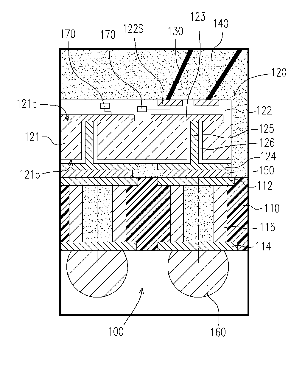
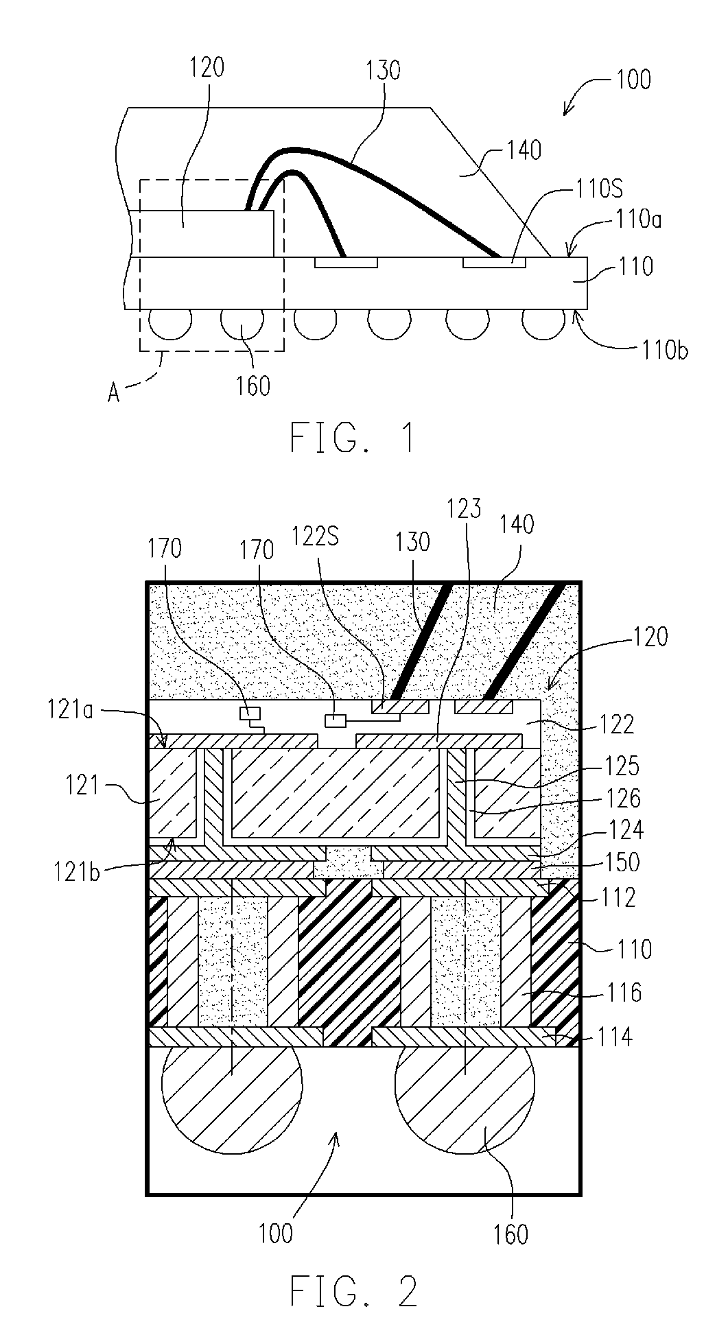
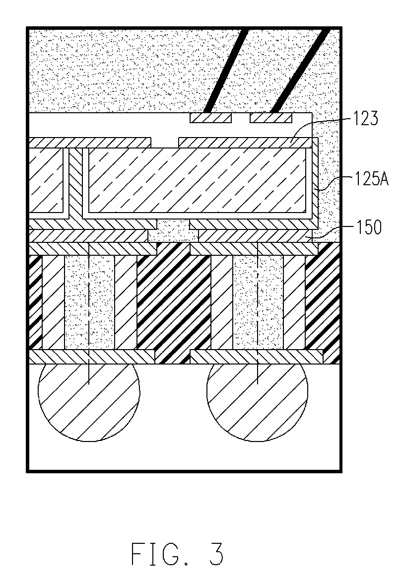
[0014]FIG. 1 is a partial sectional view of a chip package according to an embodiment of the present invention, and FIG. 2 is an enlarged view of part A of FIG. 1. Referring to FIGS. 1 and 2, a chip package 100 of an embodiment of the present invention includes a carrier 110, a chip 120, a plurality of wires 130, and an encapsulant 140. The chip 120 is disposed on the carrier 110, the wires 130 electrically connect the chip 120 to the carrier 110, and the encapsulant 140 wraps the chip 120 and the wires 130.

[0015]The chip 120 includes a semiconductor substrate 121 and an interconnection structure 122. The semiconductor substrate 121 is, for example, a silicon substrate, and has a first substrate surface 121a and a second substrate surface 121b opposite to the first substrate surface 121a, and the interconnection structure 122 is located on the first substrate surface 121a.

[0016]The interconnection structure 122 includes a plurality of chip signal pads 122s, which are composed of me...


PUM


Abstract

A chip package including a carrier, at least one chip disposed on the carrier, a plurality of wires electrically connecting the carrier and the chip, and an encapsulant wrapping the chip and the wires is provided. The chip has a semiconductor substrate, an interconnection structure, at least one first reference plane, at least one second reference plane, and at least one chip via, in which the first and second reference planes are respectively located on both sides of the semiconductor substrate, and the interconnection structure is located on the first reference plane and the semiconductor substrate. The chip via connects the first reference plane to the second reference plane. The chip package further includes at least one conductive bonding layer, which bonds the second reference plane to the carrier.

Description

CROSS-REFERENCE TO RELATED APPLICATION[0001]This application claims the priority benefit of U.S. provisional application Ser. No. 60 / 890,178, filed on Feb. 15, 2007, all disclosures are incorporated therewith.BACKGROUND OF THE INVENTION[0002]1. Field of the Invention[0003]The present invention relates to an integrated circuit (IC). More particularly, the present invention relates to a package electrically connecting two sides of a chip to a carrier carrying the chip.[0004]2. Description of Related Art[0005]Due to the development of IC process technology, signal density of a chip increases. For a packaging type of wire bonding matching with a carrier, the chip is disposed on the carrier, and a plurality of wires are used to electrically connect the chip and the carrier. However, when the signal density of the chip increases, inductance coupling between wires generated by electromagnetic effect increases, such that signals are interfered by noise and crosstalk quite seriously as trans...

Claims


Application Information

Patent Timeline
IPC IPC(8): H01L23/49
CPCH01L23/3128H01L2224/16235H01L23/49816H01L23/49827H01L24/13H01L24/16H01L24/48H01L24/73H01L2224/0401H01L2224/05599H01L2224/13099H01L2224/16H01L2224/48091H01L2224/48227H01L2224/73257H01L2924/01014H01L2924/01022H01L2924/01029H01L2924/0105H01L2924/01079H01L2924/01082H01L2924/014H01L2924/10253H01L2924/14H01L2924/15311H01L2924/19041H01L2924/19043H01L2924/19051H01L2924/30107H01L2924/3011H01L23/481H01L2224/16225H01L2924/01023H01L2924/01047H01L2924/00014H01L2224/92227H01L24/92H01L2224/13111H01L2224/45099H01L2924/0133H01L2924/0132H01L2924/181H01L2924/00012
Inventor HSU, CHI-HSING
Owner VIA TECH INC
Features
  • R&D
  • Intellectual Property
  • Life Sciences
  • Materials
  • Tech Scout
  • Unparalleled Data Quality
  • Higher Quality Content
  • 60% Fewer Hallucinations
Learn More