Active device array substrate and driving method thereof

a technology of active devices and array substrates, which is applied in static indicating devices, instruments, non-linear optics, etc., can solve the problems of their fabricating costs, reducing display quality, and increasing signal processing and fabricating costs of driving circuits, so as to reduce color shift without increasing the complexity of driving circuits thereo

Active Publication Date: 2008-08-21
AU OPTRONICS CORP
View PDF13 Cites 32 Cited by
  • Summary
  • Abstract
  • Description
  • Claims
  • Application Information

AI Technical Summary

Benefits of technology

[0011]Accordingly, the present invention is directed to an active device array substrate

Problems solved by technology

Even though color shift is reduced, such method may cause reduction in the display quality due to the RC delay effect thereof.
However, in this method, two transistors have to be formed in a single pixel unit and the number of scan lines or data lines has to be increased, therefore both the complexity of the driving circuit and the fabricating cost thereof are increased.
For example, a pixel unit

Method used


Image

  • Active device array substrate and driving method thereof
  • Active device array substrate and driving method thereof
  • Active device array substrate and driving method thereof

Examples


Embodiment Construction

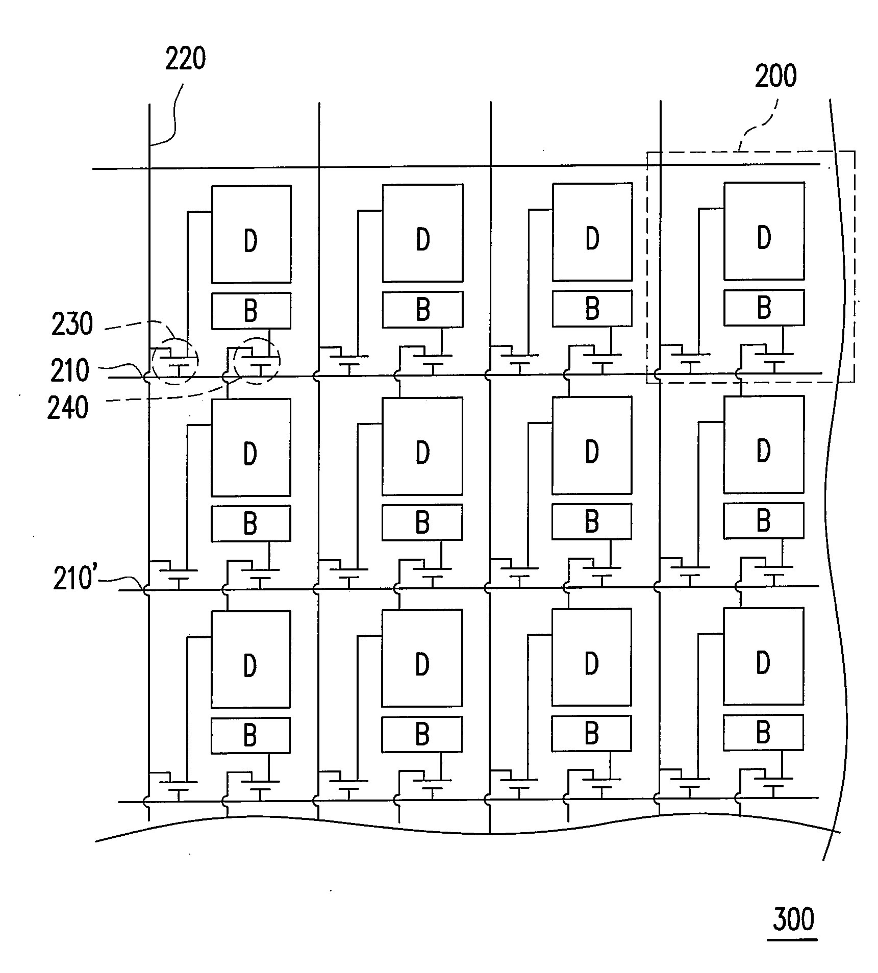
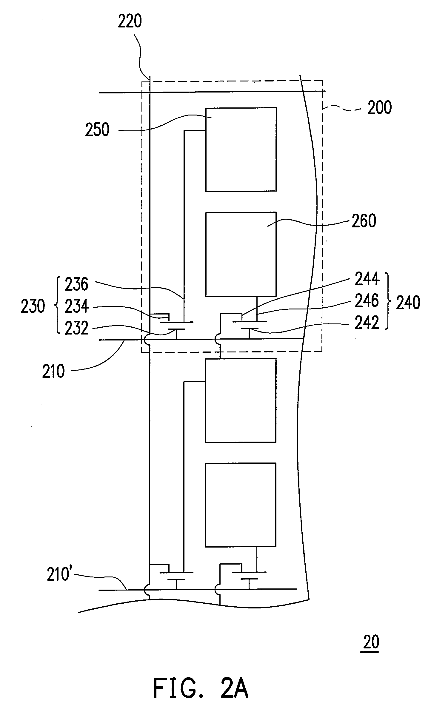
[0033]FIG. 2A is a diagram of an active device array substrate according to an embodiment of the present invention. Referring to FIG. 2A, in the present embodiment, only two pixel units 200 are illustrated in the active device array substrate 20 for the convenience of description. As shown in FIG. 2A, the active device array substrate 20 includes a plurality of scan lines 210, a plurality of data lines 220, and a plurality of pixel units 200. The pixel units 200 are connected to the scan lines 210 and data lines 220 correspondingly, and each pixel unit 200 includes a first active device 230, a second active device 240, a first pixel electrode 250, and a second pixel electrode 260. In the present embodiment, the first active device 230 and the second active device 240 may be a-Si thin film transistors (TFTs); however, the first active device 230 and the second active device 240 may also be poly-Si TFTs or other type of switches. Besides, in the present embodiment, the first active de...


PUM


Abstract

An active device array substrate including a plurality of scan lines, data lines and pixel units is provided. The pixel units are connected to the scan lines and data lines correspondingly, and each pixel unit includes a first active device, a second active device, a first pixel electrode, and a second pixel electrode. The first active device has a first gate, a first source connected to one of the data lines, and a first drain. The second active device has a second gate, a second source, and a second drain, wherein the first and the second gates are connected to the same scan line. The first and the second pixel electrodes are connected to the first drain and the second drain, respectively. The second source of each pixel unit is connected to the first pixel electrode of an adjacent pixel unit controlled by the next scan line.

Description

CROSS-REFERENCE TO RELATED APPLICATION[0001]This application claims the priority benefit of Taiwan application serial no. 96105745, filed Feb. 15, 2007. All disclosure of the Taiwan application is incorporated herein by reference.BACKGROUND OF THE INVENTION[0002]1. Field of the Invention[0003]The present invention relates to a liquid crystal display (LCD) panel. More particularly, the present invention relates to an active device array substrate and a driving method thereof.[0004]2. Description of Related Art[0005]Presently, the performance of thin film transistor liquid crystal display (TFT-LCD) is proceeding towards high contrast ratio, no gray level inversion, low color shift, high luminance, high color richness, high color saturation, quick response, and wide viewing angle etc. Existing techniques for achieving wide viewing angle include twisted nematic (TN) liquid crystal plus wide viewing film, in-plane switching (IPS) LCD, fringe field switching LCD, and multi-domain vertical...

Claims


Application Information

Patent Timeline
IPC IPC(8): G02F1/136G02F1/1343
CPCG02F1/13624G02F2001/134345G09G3/3607G09G3/3648G09G2320/028G09G2300/0443G09G2310/02G09G2310/0205G09G3/3659G02F1/134345
Inventor SU, JENN-JIASU, TING-WEIHSU, WEN-HAO
Owner AU OPTRONICS CORP
Why Eureka
Try Eureka