Integrated multilayer chip capacitor module and integrated circuit apparatus having the same

a multi-layer chip capacitor and integrated circuit technology, which is applied in the direction of fixed capacitor details, fixed capacitors, semiconductor/solid-state device details, etc., can solve the problems of multi-terminal multi-layer capacitors that cannot be mounted at a higher density and with a lower esl, and achieve better decoupling effects and low impedance

Active Publication Date: 2008-08-28
SAMSUNG ELECTRO MECHANICS CO LTD
View PDF9 Cites 7 Cited by
  • Summary
  • Abstract
  • Description
  • Claims
  • Application Information

AI Technical Summary

Benefits of technology

[0011]An aspect of the present invention provides an integrated chip capacitor module which has lower impedance at a high and low frequency to achieve better decoupling effects in a broader frequency range, and an integrated circuit apparatus having the same.

Problems solved by technology

In the multilayer chip capacitor module of FIG. 1, ‘two terminal’ capacitors can be integrated into a single module structure, but ‘multi-terminal’ multi-layer capacitors cannot be mounted at a higher density and with lower ESL.

Method used


Image

  • Integrated multilayer chip capacitor module and integrated circuit apparatus having the same
  • Integrated multilayer chip capacitor module and integrated circuit apparatus having the same
  • Integrated multilayer chip capacitor module and integrated circuit apparatus having the same

Examples


##ventive example 1

Inventive Example 1

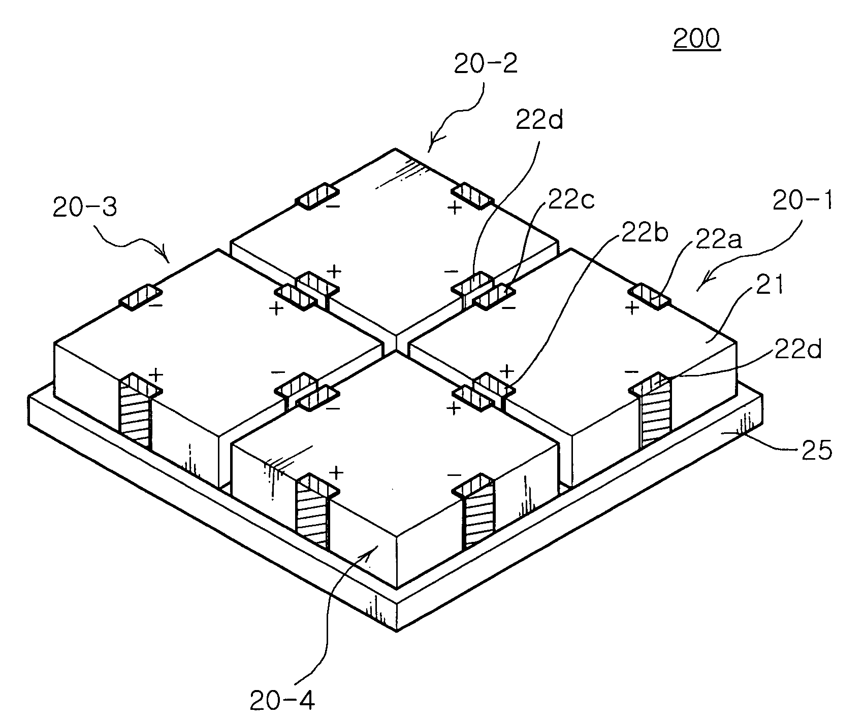
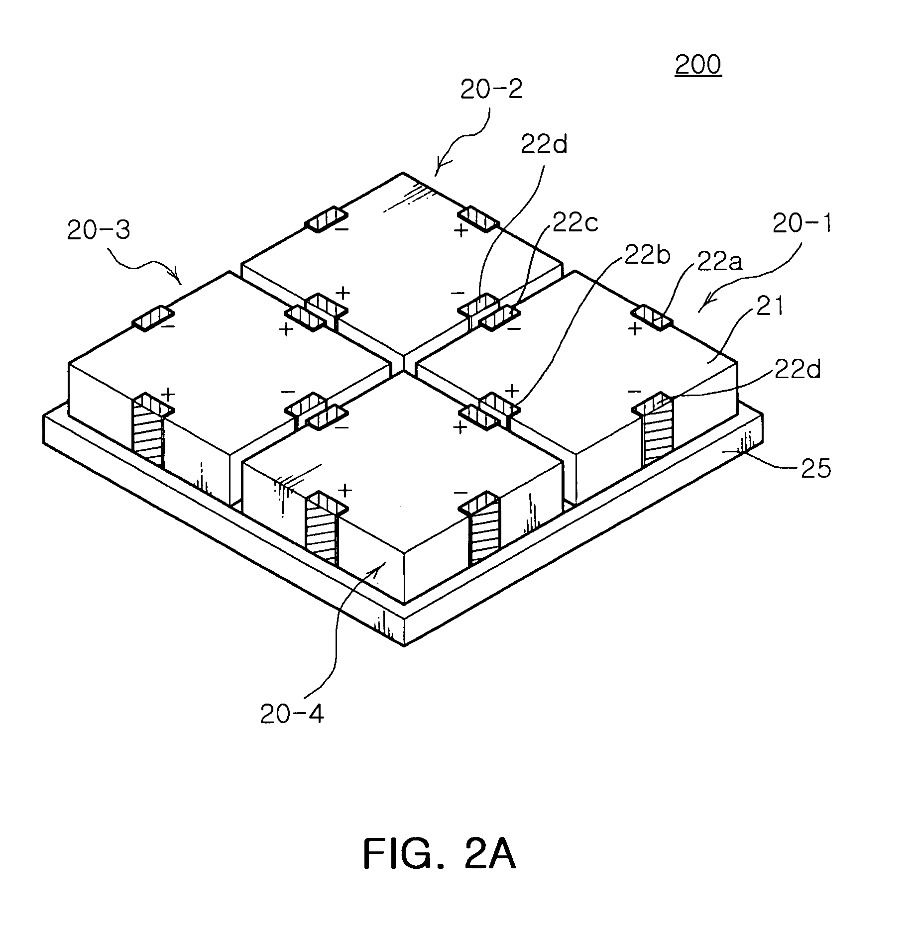
[0065]In a capacitor module of Inventive Example 1, four multilayer chip capacitors with a size of 1005 (1.0 mm×0.5 mm) were arranged close to one another and co-planar with one another in a 2×2 matrix. The chip capacitors were mounted on a capacitor body (see reference numeral 25 of FIG. 2A). Each of the capacitors is a multi-terminal and low-ESL capacitor having a capacitance of 2.2 μF. This capacitor module was mounted on a PCB.

[0066]To compare with characteristics of Inventive Example 1, Comparative Example 1 was prepared, in which four multilayer capacitors with a same size of 1005 were mounted discretely on a PCB in a conventional mounting method. The discrete capacitors mounted according to Comparative Example 1 were connected in parallel with one another through a wiring pattern previously formed on the PCB.

[0067]Table 1 below shows total occupied area (total mounting area) and capacitance density measured in Inventive Example 1 and Comparative Example 1, ...

##ventive example 2

Inventive Example 2

[0069]Apart from Inventive Example 1, capacitors with a 1005 size and 100pH ESL were employed to obtain a maximum number of mountable capacitors in a limited total mounting area (10 mm×10 mm) and measure total inductance when the maximum number of capacitors were mounted.

[0070]In Inventive Example 2, the capacitor module shown in FIG. 2A was adopted to mount the capacitors on the PCB. In Comparative Example 2, the capacitors were mounted discretely on the PCB by a conventional mounting method (see Comparative Example 1, a different number of capacitors from Comparative Example 1).

TABLE 2Maximum number ofmountablecapacitorsTotal inductanceComparative Example 2801.25 pH(Discrete capacitors)Inventive Example 21040.96 pH(Integrated capacitormodule)

[0071]As noted in Table 2, when compared with Comparative Example 2 where the capacitors are arranged discretely, in the capacitor module of Inventive Example 2, a greater number of capacitors can be mounted in an identical ...


PUM


Abstract

An integrated multilayer chip capacitor module including: plurality of multilayer chip capacitors arranged close to one another and co-planar with one another; and a capacitor support accommodating the multilayer chip capacitors, wherein each of the multilayer chip capacitors includes a rectangular parallelepiped capacitor body and a plurality of first and second external electrodes formed on at least two sides of the capacitor body, and the external electrodes on adjacent sides of adjacent ones of the multilayer chip capacitor in the capacitor support are electrically connected to each other by a conductive adhesive material.

Description

CROSS-REFERENCE TO RELATED APPLICATIONS[0001]This application claims the priority of Korean Patent Application No. 2007-19232 filed on Feb. 26, 2007, in the Korean Intellectual Property Office, the disclosure of which is incorporated herein by reference.BACKGROUND OF THE INVENTION[0002]1. Field of the Invention[0003]The present invention relates to an integrated multilayer chip capacitor module and an integrated circuit apparatus having the capacitor module, and more particularly, an integrated multilayer chip capacitor module which has capacitors mounted at a higher density to reduce power network impedance in high and low frequency regions, and a micro-processor unit (MPU) integrated circuit apparatus having the same.[0004]2. Description of the Related Art[0005]In general, a multilayer chip capacitor has internal electrodes of different polarities deposited alternately to interpose each of dielectric layers. This multilayer chip capacitor advantageously ensures a smaller size, a h...

Claims


Application Information

Patent Timeline
Patent Type & Authority Applications(United States)
IPC IPC(8): H01G4/228
CPCH01G2/06H01G4/232H01G4/38H01L23/50H01L2924/0002H01L2924/00H01G4/005H01G4/30
Inventor LEE, BYOUNG HWAWI, SUNG KWONPARK, SANG SOOPARK, MIN CHEOLPARK, DONG SEOK
Owner SAMSUNG ELECTRO MECHANICS CO LTD
Why Eureka
Try Eureka