Semiconductor device test structures and methods

a technology of semiconductor devices and test structures, applied in semiconductor/solid-state device testing/measurement, semiconductor operation lifetime testing, instruments, etc., can solve problems such as interference of electrical current flow, small conductive features of semiconductor devices, and break or gap in conductive materials

Active Publication Date: 2008-08-28
INFINEON TECH AG
View PDF31 Cites 19 Cited by
  • Summary
  • Abstract
  • Description
  • Claims
  • Application Information

AI Technical Summary

Benefits of technology

[0012]These and other problems are generally solved or circumvented, and technical advantages are generally achieved, by preferred embodiments of the present invention, which provide improved structures and methods for testing and measuring electromigration and electromigration-related parameters in semiconductor devices.

Problems solved by technology

Electromigration is a phenomenon that occurs in conductive materials that can cause problems in semiconductor devices having small conductive features.
Over time, the movement of atoms from their original positions due to electromigration can cause a break or gap in the conductive material, preventing or hindering the flow of electrical current.
Electromigration can also cause the atoms of a conductor to pile up and drift toward other nearby conductors, creating an unintended electrical connection known as a hillock or whisker failure, or a short circuit.
Both voids and hillock failures can lead to a malfunction of an integrated circuit.
Electromigration is particularly a problem in applications where high direct current densities are used.
With increasing miniaturization, the probability of failure due to electromigration increases in semiconductor devices, because smaller conductive lines have increased power density and current density.
Electromigration can lead to the eventual loss of one or more connections, and to the intermittent failure and / or eventually permanent failure of an entire circuit.
Electromigration is an inherent limitation for very large scale integration (VLSI) interconnect systems, because electromigration reliability issues limit current density increase in ever-shrinking VLSI circuitry.
One key cost issue facing semiconductor device designers is the acceleration of electromigration testing times, which currently may range from several hours to several days, for example.
Temperature and current density are two factors involved in the acceleration of electromigration testing times. Both factors are limited: increased temperature can initiate other non-electromigration degradation mechanisms, while increased current density tends to cause temperature inhomogeneities in test structures, deteriorating or inhibiting the electromigration assessment.
Via and contact issues may be independent from conductive line issues and have become critical issues for Cu and AlCu interconnect systems, for example.

Method used


Image

  • Semiconductor device test structures and methods
  • Semiconductor device test structures and methods
  • Semiconductor device test structures and methods

Examples


Embodiment Construction

[0028]The making and using of the presently preferred embodiments are discussed in detail below. It should be appreciated, however, that the present invention provides many applicable inventive concepts that can be embodied in a wide variety of specific contexts. The specific embodiments discussed are merely illustrative of specific ways to make and use the invention, and do not limit the scope of the invention.

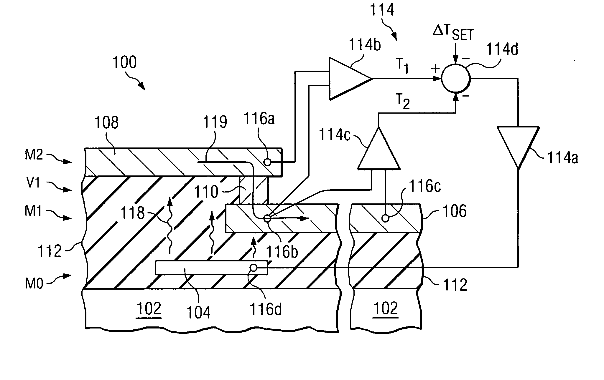
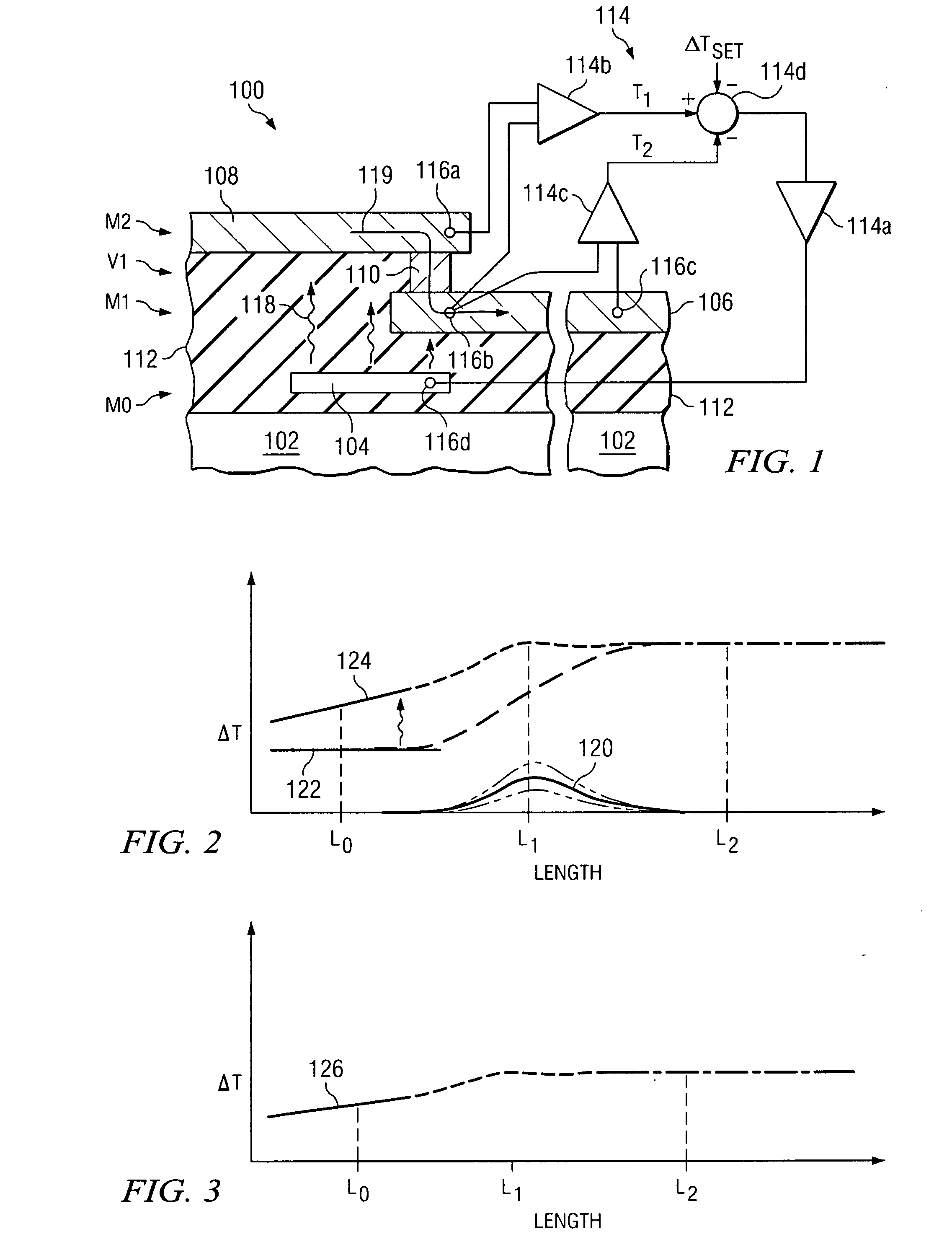
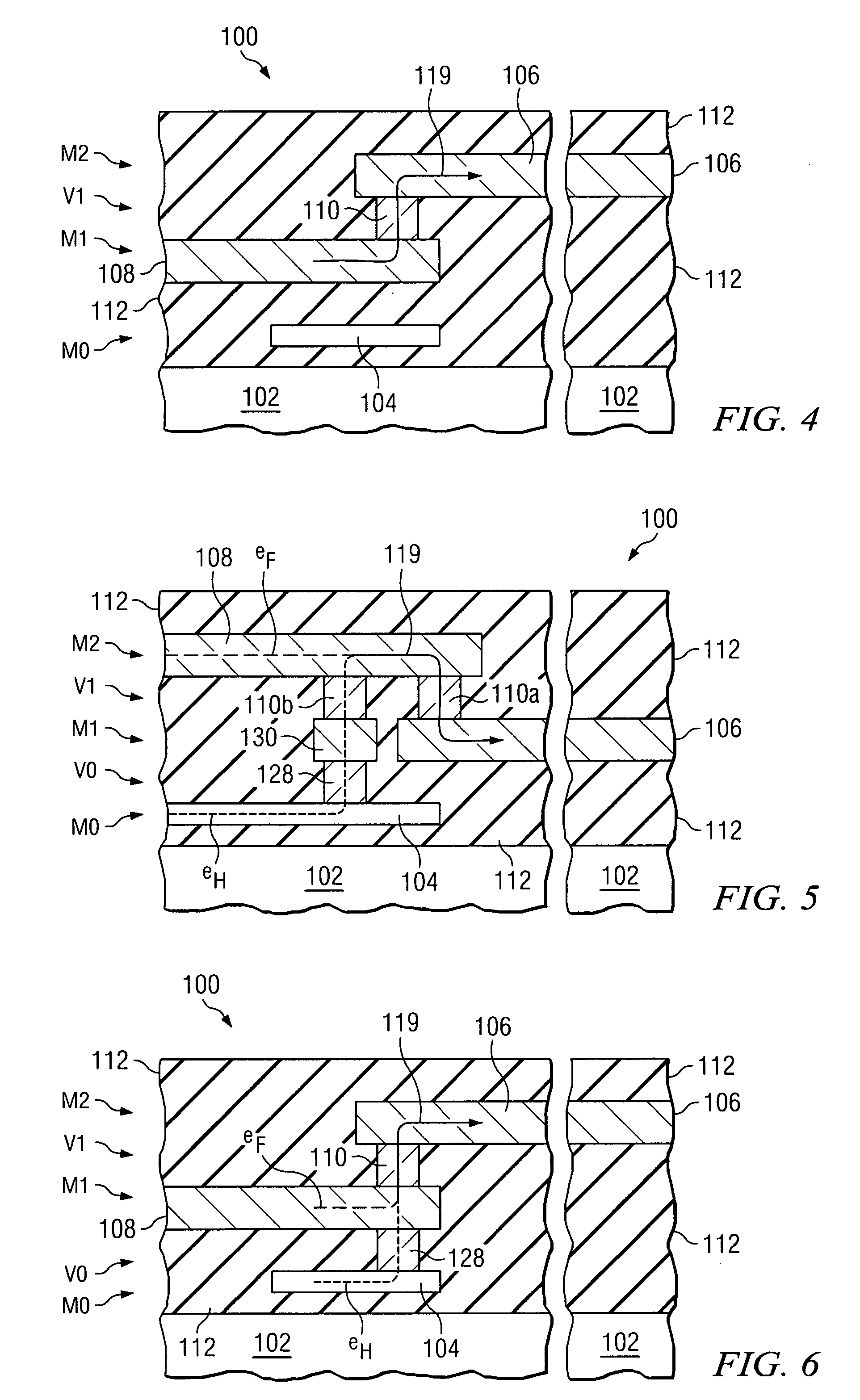
[0029]Conventional via-line test structures for measuring electromigration typically comprise a feed line for supplying current and a stress line that is used for making measurements of electromigration. The stress line is formed in a different conductive material layer than the feed line, and the feed line is connected to the stress line for the electromigration measurements by one or more vias disposed between the two conductive material layers. In order to accelerate the test time of such conventional test structures, the test current is often increased. However, increasin...


PUM


Abstract

Semiconductor device test structures and methods are disclosed. In a preferred embodiment, a test structure includes a feed line, a stress line disposed proximate the feed line, and a conductive feature disposed between the stress line and the feed line. The test structure includes a temperature adjuster proximate at least the conductive feature, and at least one feedback device coupled to the temperature adjuster and at least the conductive feature.

Description

CROSS-REFERENCE TO RELATED APPLICATIONS[0001]This application relates to the following co-pending and commonly assigned patent application: Ser. No. ______, attorney docket no. 2006 P 54041 US, filed on Feb. 6, 2007, entitled, “Semiconductor Device Test Structures and Methods,” which application is hereby incorporated herein by reference.TECHNICAL FIELD[0002]The present invention relates generally to the fabrication of semiconductor devices, and more particularly to test structures and methods for semiconductor devices.BACKGROUND[0003]Generally, semiconductor devices are used in a variety of electronic applications, such as computers, cellular phones, personal computing devices, and many other applications. Home, industrial, and automotive devices that in the past comprised only mechanical components now have electronic parts that require semiconductor devices, for example.[0004]Semiconductor devices are manufactured by depositing many different types of material layers over a semic...

Claims


Application Information

Patent Timeline
Patent Type & Authority Applications(United States)
IPC IPC(8): H01L21/66G01R31/26H01L23/58
CPCG01R31/2642G01R31/2831H01L22/34G01R31/2879G01R31/2858
Inventor WALTER, WOLFGANG
Owner INFINEON TECH AG
Why Eureka
Try Eureka