Yield analysis and improvement using electrical sensitivity extraction

a technology of electrical sensitivity and yield analysis, applied in the direction of stochastic cad, cad techniques, instruments, etc., can solve the problems of different types of circuit failure, short defects, and increasing difficulty for semiconductor designers to estimate and realize device yields

Inactive Publication Date: 2008-08-28
NXP USA INC
View PDF15 Cites 33 Cited by
  • Summary
  • Abstract
  • Description
  • Claims
  • Application Information

AI Technical Summary

Problems solved by technology

As semiconductor device geometries continue to shrink and new process materials are adopted, it is increasingly difficult for semiconductor designers to estimate and realize device yields which traditionally have been limited primarily by defect density, but which is now impacted greatly by the interaction of process-related deviations with design elements.
Defects can cause different types of circuit failures.
For example, “short” defects are caused by extra material that is formed to connect or “short” different conducting regions, which can occur when shapes are printed larger than designed during the manufacturing process.
As another example, “open” defects can occur when shapes are printed smaller than designed during the manufacturing process and when non-conductive particles or contaminants are formed in a conducting region to create an open circuit.
While the CAA yield model is useful for predicting a yield value that can be used as a tool to control chip manufacturing costs, the CAA yield model has a built-in error in failing to properly account for the effects of “partial” open and short defects.
If the CAA yield model accounts for this partial open defect as a yield loss, then this results in a false yield loss prediction, which in turn can lead wasted efforts to correct false yield issues.
Conversely, in the case where a conductive line is only partially blocked by a contaminant / particle so that the conductive line is insufficiently conductive, but the CAA yield model waives partial open defect (i.e., does not include it as a yield loss), then this results in a yield loss not being detected, which can result in the tape out of low yield products.

Method used


Image

  • Yield analysis and improvement using electrical sensitivity extraction
  • Yield analysis and improvement using electrical sensitivity extraction
  • Yield analysis and improvement using electrical sensitivity extraction

Examples


Embodiment Construction

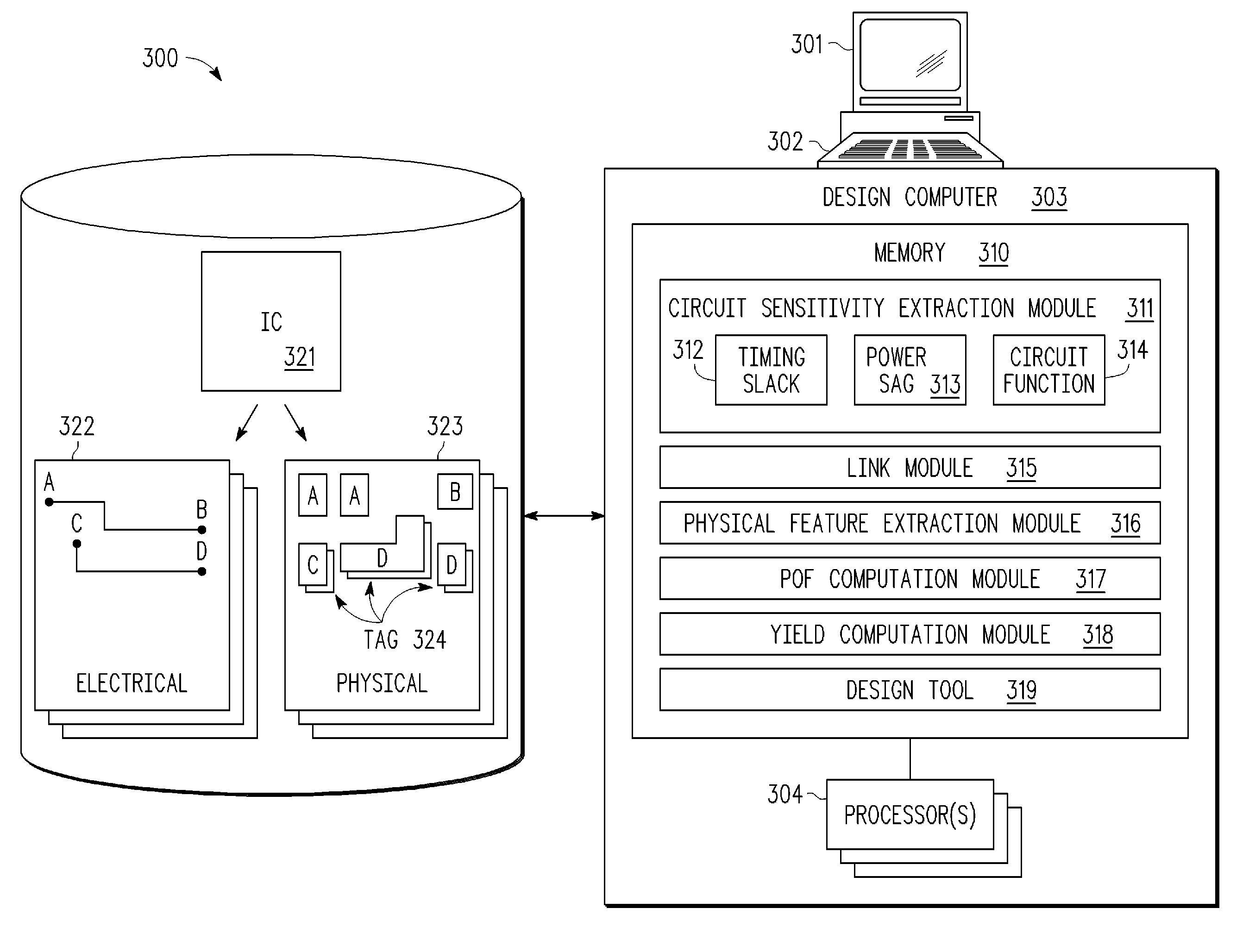
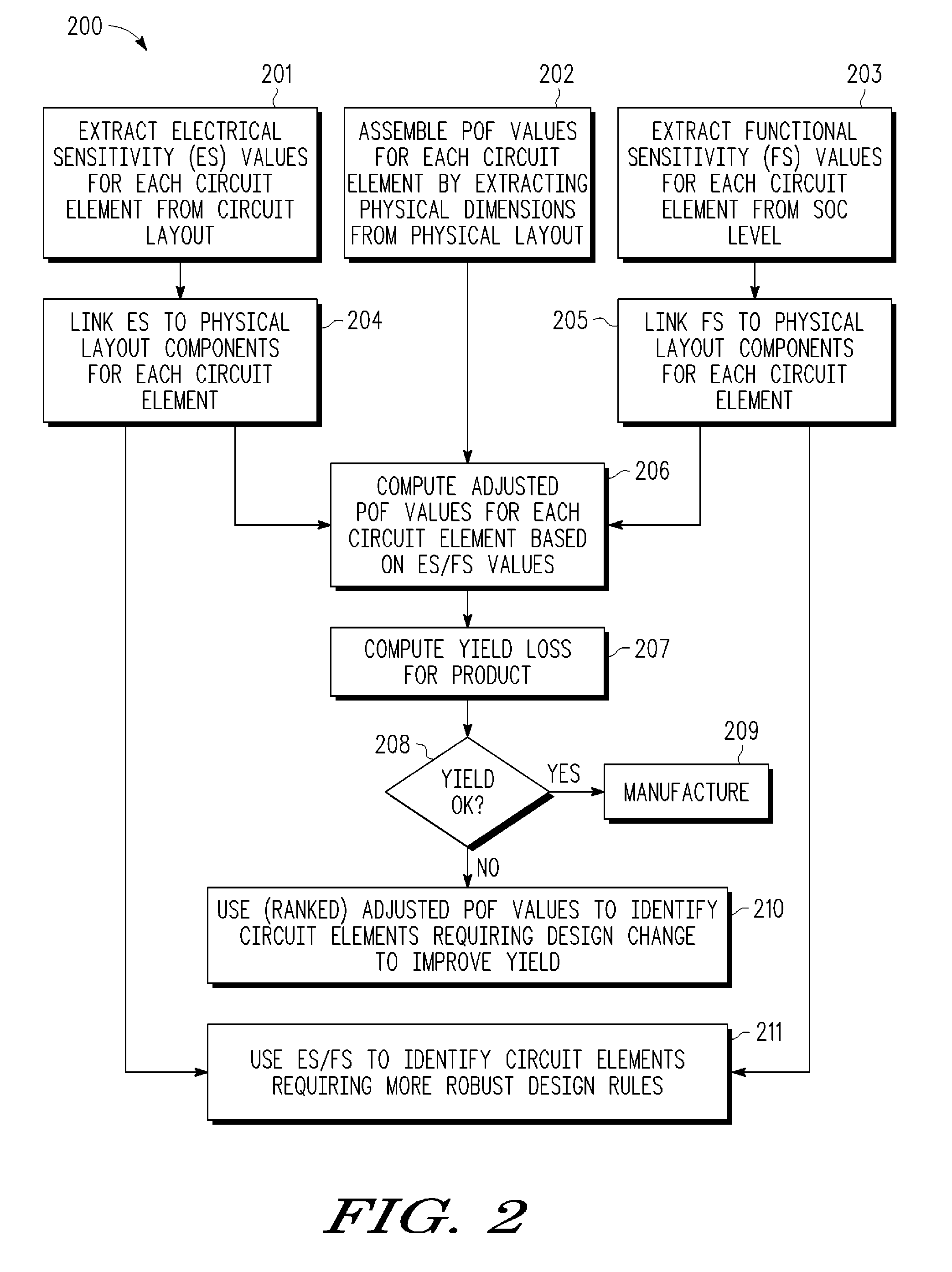
[0013]A method and apparatus are described for determining an accurate yield prediction for an integrated circuit by combining conventional yield loss analysis (such as extracted from physical dimension information concerning a circuit layout) with extracted electrical sensitivity and / or functional sensitivity information for circuit elements (such as nets connecting logic blocks or other signal lines) to obtain an actual performance-based probability of failure (POF) for the overall circuit. As a preliminary step, electrical and / or functional sensitivity information is extracted for one or more circuit elements. In various embodiments, electrical sensitivity information can be a function of the timing slack associated with the circuit element, where the timing slack is a measure of how quickly the circuit element must deliver a signal, or in other words, how much time there is between when a signal arrives at its destination and when the clock at the destination is triggered. Thus,...


PUM


Abstract

A method and apparatus are described for determining an accurate yield prediction for an integrated circuit by combining conventional yield loss analysis (such as extracted from physical dimension information concerning a circuit layout) with extracted electrical sensitivity and / or functional sensitivity information for circuit elements (such as nets connecting logic blocks or other signal lines) to obtain an actual performance-based probability of failure (POF) for the overall circuit.

Description

BACKGROUND OF THE INVENTION[0001]1. Field of the Invention[0002]The present invention is directed in general to the field of integrated circuit design. In one aspect, the present invention relates to a method of predicting manufacturing yield of a proposed integrated circuit design.[0003]2. Description of the Related Art[0004]As semiconductor device geometries continue to shrink and new process materials are adopted, it is increasingly difficult for semiconductor designers to estimate and realize device yields which traditionally have been limited primarily by defect density, but which is now impacted greatly by the interaction of process-related deviations with design elements. One approach for predicting yield, called the critical area analysis (CAA), uses a “critical area” of an integrated circuit layout as a measure to reflect the sensitivity of the layout to defects created occurring during the manufacturing process by particles, such as dust and other contaminants in materials...

Claims


Application Information

Patent Timeline
Patent Type & Authority Applications(United States)
IPC IPC(8): G06F17/50
CPCG06F2217/10G06F17/5068G06F30/39G06F2111/08
Inventor RIVIERE-CAZAUX, LIONEL J.
Owner NXP USA INC
Why Eureka
Try Eureka