Image sensor and method of fabricating the same

Inactive Publication Date: 2008-09-18
SAMSUNG ELECTRONICS CO LTD
View PDF4 Cites 17 Cited by
  • Summary
  • Abstract
  • Description
  • Claims
  • Application Information

AI Technical Summary

Benefits of technology

[0008]Exemplary embodiments of the present invention provide an image sensor

Problems solved by technology

If the integration density of pixels is increased according to an enhanced resolution, however, an area of a photoelectric converter in each unit pixel is reduced, thereby deteriorating the sensitivity and decreasing an amount of saturation signals.
To this end, however, the method requires excessive ion implantati

Method used


Image

  • Image sensor and method of fabricating the same
  • Image sensor and method of fabricating the same
  • Image sensor and method of fabricating the same

Examples


Example

[0029]Exemplary embodiments of the present invention will now be described more fully with reference to the accompanying drawings, in which exemplary embodiments of the invention are shown. The invention may, however, be embodied in many different forms and should not be construed as being limited to the exemplary embodiments set forth herein; rather, these exemplary embodiments are provided so that this disclosure will be thorough and complete, and will fully convey the concept of the invention to those of ordinary skill in the art.

[0030]In some exemplary embodiments, well-known processing processes, well-known structures, and well-known technologies will not be specifically described in detail in order to avoid an ambiguous interpretation of the present invention.

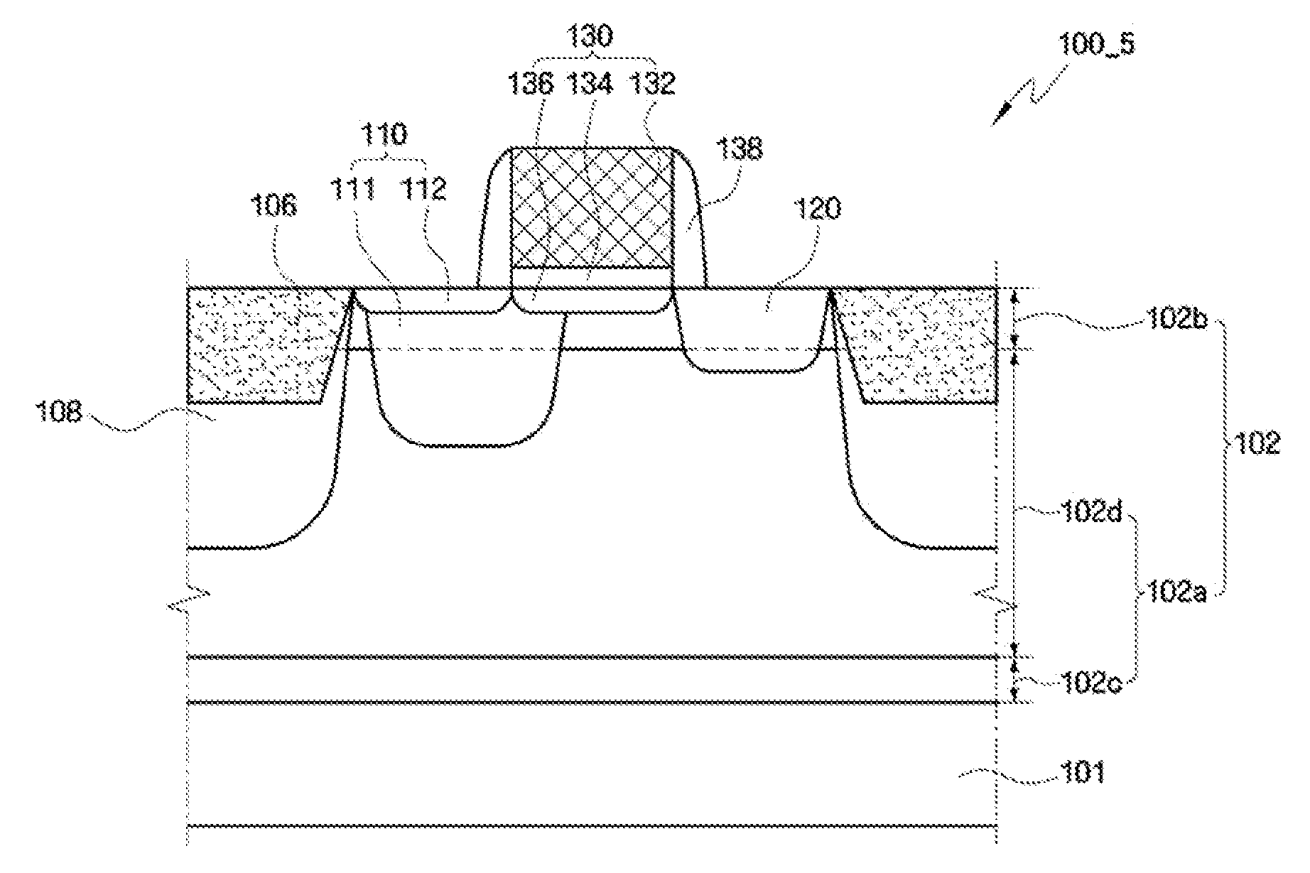
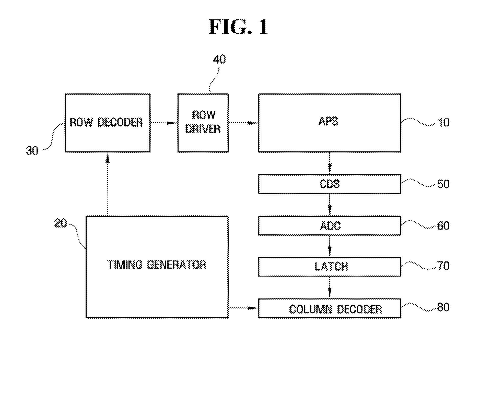
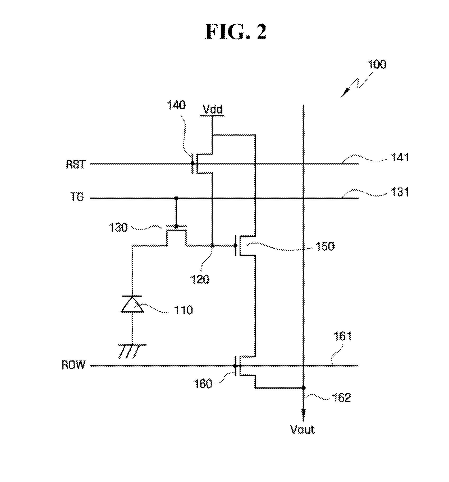
[0031]Image sensors according to exemplary embodiments of the present invention include charge coupled device (CCD) image sensors and complementary metal oxide semiconductor (CMOS) image sensors. CCD image sensors have le...


PUM


Abstract

An image sensor with sufficient photoelectric conversion capacity and enhanced reliability and a method of fabricating the same, in which the image sensor includes a bare substrate; an epitaxial layer disposed on the bare substrate and including a first impurity distribution region of a first conductivity type, which is formed on the bare substrate, and a second impurity distribution region of a second conductivity type, which is formed on the first impurity distribution region; and a charge collection well formed within the epitaxial layer and at least partially doped with third impurities of the second conductivity type, wherein the charge collection well occupies the first impurity distribution region and the second impurity distribution region and represents the second conductivity type as a whole.

Description

[0001]This application claims priority from Korean Patent Application No. 10-2007-026276 filed on Mar. 16, 2007 in the Korean Intellectual Property Office, the disclosure of which is incorporated herein by reference in its entirety.BACKGROUND OF THE INVENTION[0002]1. Technical Field[0003]The present disclosure relates to an image sensor and a method of fabricating the same and, more particularly, to an image sensor with sufficient photoelectric conversion capacity and enhanced reliability and a method of fabricating the same.[0004]2. Discussion of Related Art[0005]With recent advancements in the computer and communication industries, the demands for image sensors with enhanced performance are increasing in various fields such as digital cameras, camcorders, personal communication systems, game devices, security cameras, and micro-cameras for medical use.[0006]Metal oxide semiconductor (MOS) image sensors can be driven using a simple driving method and can be implemented using variou...

Claims


Application Information

Patent Timeline
IPC IPC(8): H01L31/113H01L21/00
CPCH01L27/14609H01L27/14689H01L27/1463H01L27/146
Inventor LEE, JONG-MINSHIN, JONG-CHEOLPARK, DOO-CHEOLKOO, JEONG-HOONLIM, HEE-YONG
Owner SAMSUNG ELECTRONICS CO LTD
Why Eureka
Try Eureka