Lazy Susan Tool Layout for Light-Activated ALD

Inactive Publication Date: 2008-09-18
TOKYO ELECTRON LTD
View PDF5 Cites 15 Cited by
  • Summary
  • Abstract
  • Description
  • Claims
  • Application Information

AI Technical Summary

Benefits of technology

[0004]An objective of the present inventi

Problems solved by technology

The technology is relatively new, and few known processes provide the efficiency desirable for com

Method used


Image

  • Lazy Susan Tool Layout for Light-Activated ALD
  • Lazy Susan Tool Layout for Light-Activated ALD
  • Lazy Susan Tool Layout for Light-Activated ALD

Examples


Example

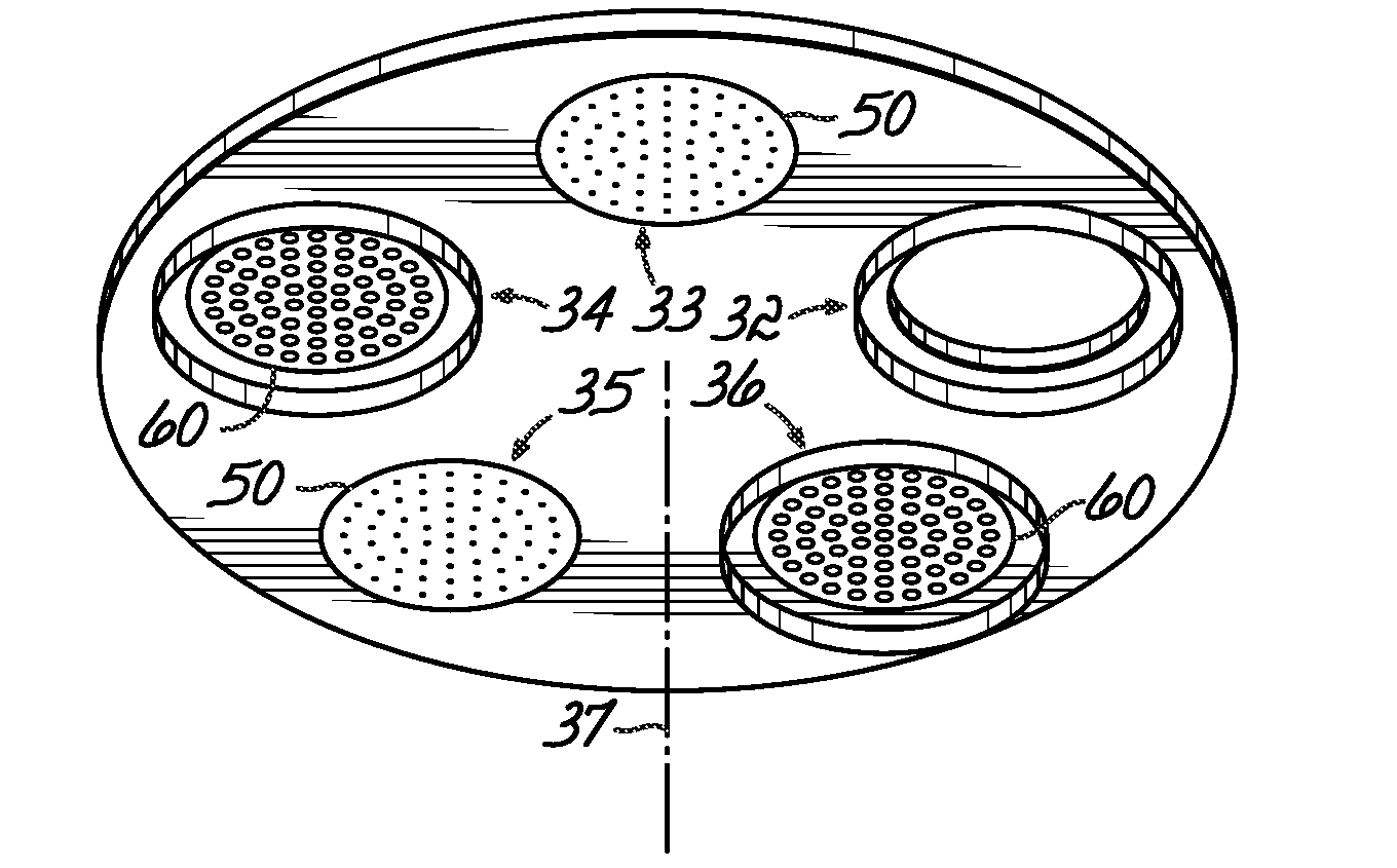
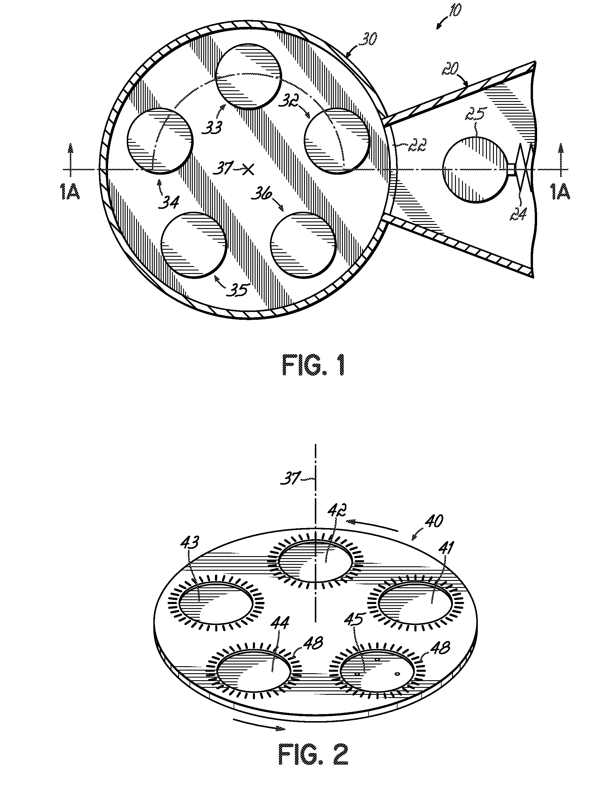
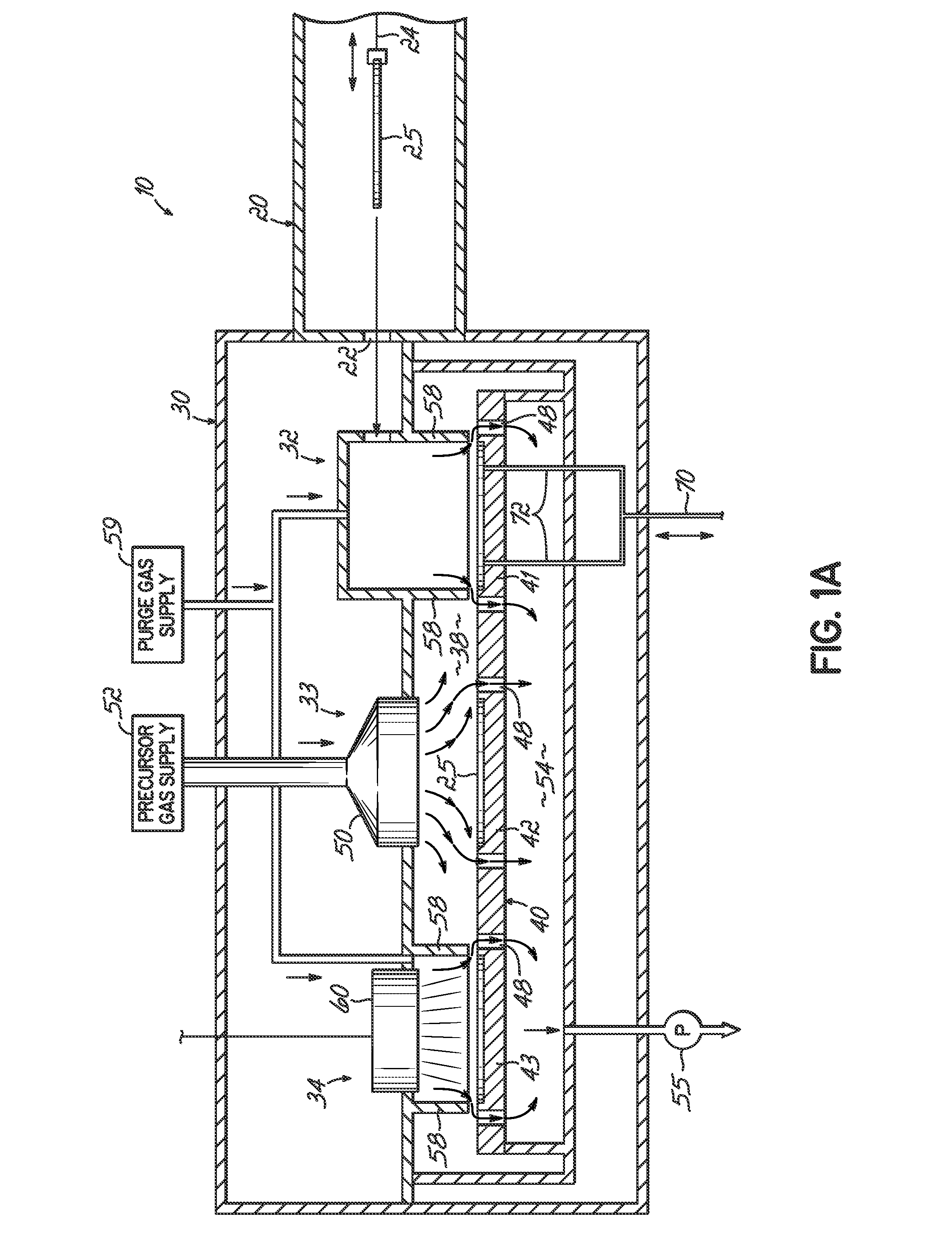
[0020]FIG. 1 is a diagrammatic top view of a portion of a semiconductor wafer processing tool 10 that includes a transfer module 20 and an atomic layer deposition (ALD) module 30. The ALD module 30 is coupled to the transfer module 20 through a gate valve 22. The transfer module 20 has a transfer arm 24 that loads wafers 25 into, and removes wafers 25 from, a wafer transfer station 32 of the ALD module 30, as well as to and from other modules (not shown) of the processing tool 10.

[0021]The ALD module 30 includes, in addition to the wafer transfer station 32, two precursor deposition stations 33 and 35, and two light activation stations 34 and 36. The stations 32-36 are located at equally angularly-spaced positions, at equal radii from a vertical centerline 37, in an ALD processing chamber 38 of the ALD module 30. The stations are arranged around the centerline 37 in the chamber 38 in the order of: transfer station 32, deposition station 33, activation station 34, deposition station ...


PUM


Abstract

An atomic layer deposition (ALD) module is provided with a rotatable carrier plate that holds a plurality of wafer holders at equally spaced angular positions. The plate is rotated to carry the wafers through a plurality of processing stations arranged at similarly equally spaced angular intervals around the axis of rotation of the rotatable plate. Rotation of the carrier plate carries a plurality of substrates successively through a plurality of pairs of stations, each pair including a precursor deposition station and a light activation station. A plurality of rotations may be used to apply a complete ALD film on the substrates. Wafers in different holders on the carrier are simultaneously processed in different stations, with some having precursor deposited thereon and others having the precursor thereon activated by light. One or more transfer stations can be included for loading or unloading wafers to and from the carrier. The number of holders on the carrier equals the number of stations in the module. Curtains and purge gas flow direction features keep precursor gas from the deposition stations from entering the activation or transfer stations.

Description

[0001]This invention relates to processing tool configurations and cycling for Atomic Layer Deposition (ALD).BACKGROUND OF THE INVENTION[0002]In atomic layer deposition (ALD), very thin films, for example of metal, are deposited on a substrate by rapid cycling of repeated depositions of a precursor with each deposition followed by an activation step. Often twenty or more cycles are required to successfully deposit a film. The technology is relatively new, and few known processes provide the efficiency desirable for commercial ALD. All such known processes have unsolved problems that interfere with process efficiency.[0003]Accordingly, efficient ALD processes arc needed.SUMMARY OF THE INVENTION[0004]An objective of the present invention is to provide an efficient ALD process.[0005]A further objective of the present invention is to provide an ALD process in which process parameters can be changed quickly going from deposition to activation to deposition, etc. on a given wafer.[0006]A ...

Claims


Application Information

Patent Timeline
IPC IPC(8): C23C16/48C23C16/44
CPCC23C16/45551
Inventor VUKOVIC, MIRKO
Owner TOKYO ELECTRON LTD
Why Eureka
Try Eureka