

Method of manufacturing semiconductor device and control system
a control system and semiconductor technology, applied in the direction of semiconductor/solid-state device testing/measurement, electrical equipment, basic electric elements, etc., can solve the problems of serious degradation of the operation efficiency of the apparatus, increase in so-called down time, and wide width of the obtainable recesses, so as to reduce the dimensional shift (l2l1) and reduce the dimensional shift (l2l1)
Inactive Publication Date: 2008-09-18
RENESAS ELECTRONICS CORP
View PDF3 Cites 3 Cited by
- Summary
- Abstract
- Description
- Claims
- Application Information
AI Technical Summary
Benefits of technology
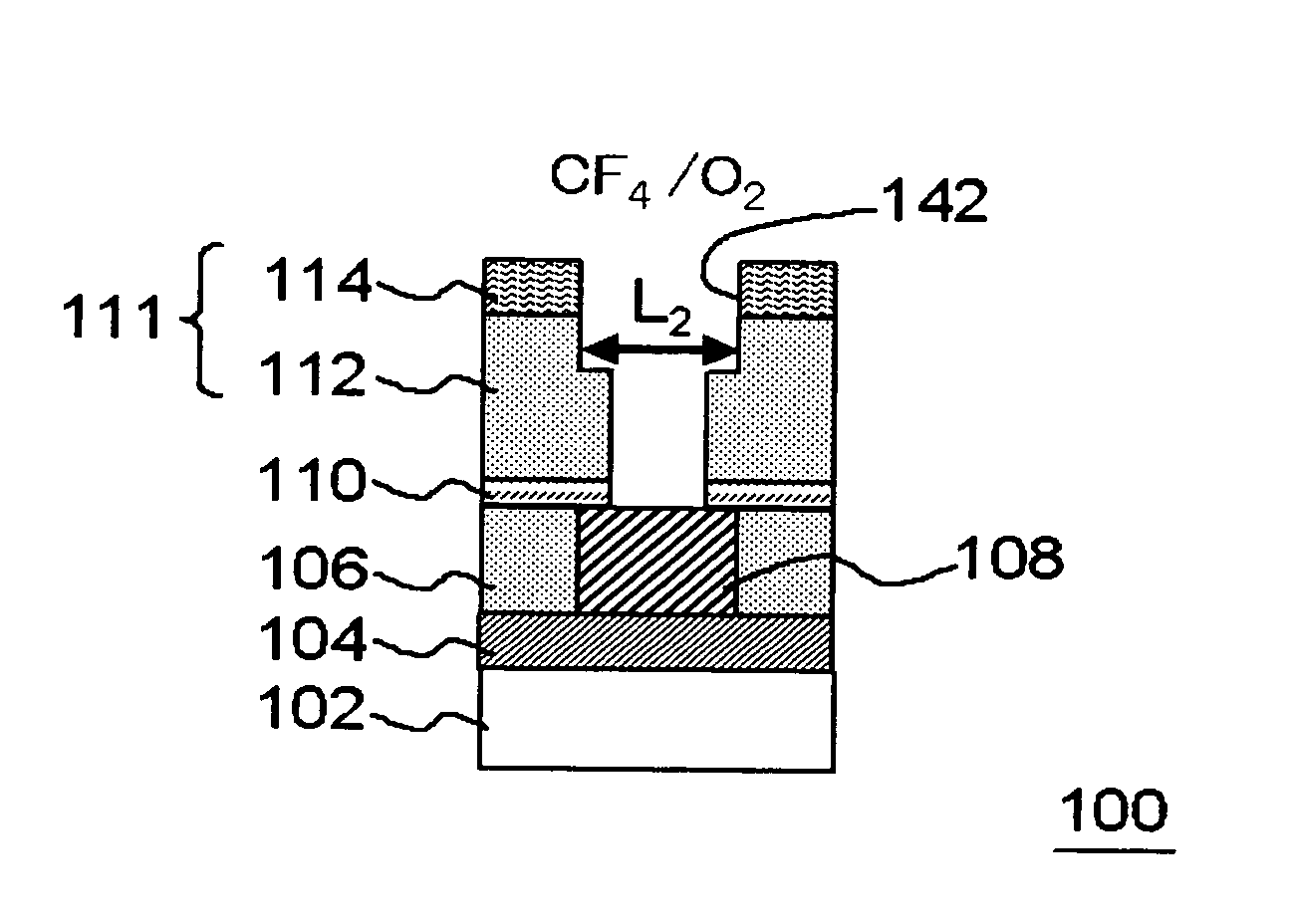
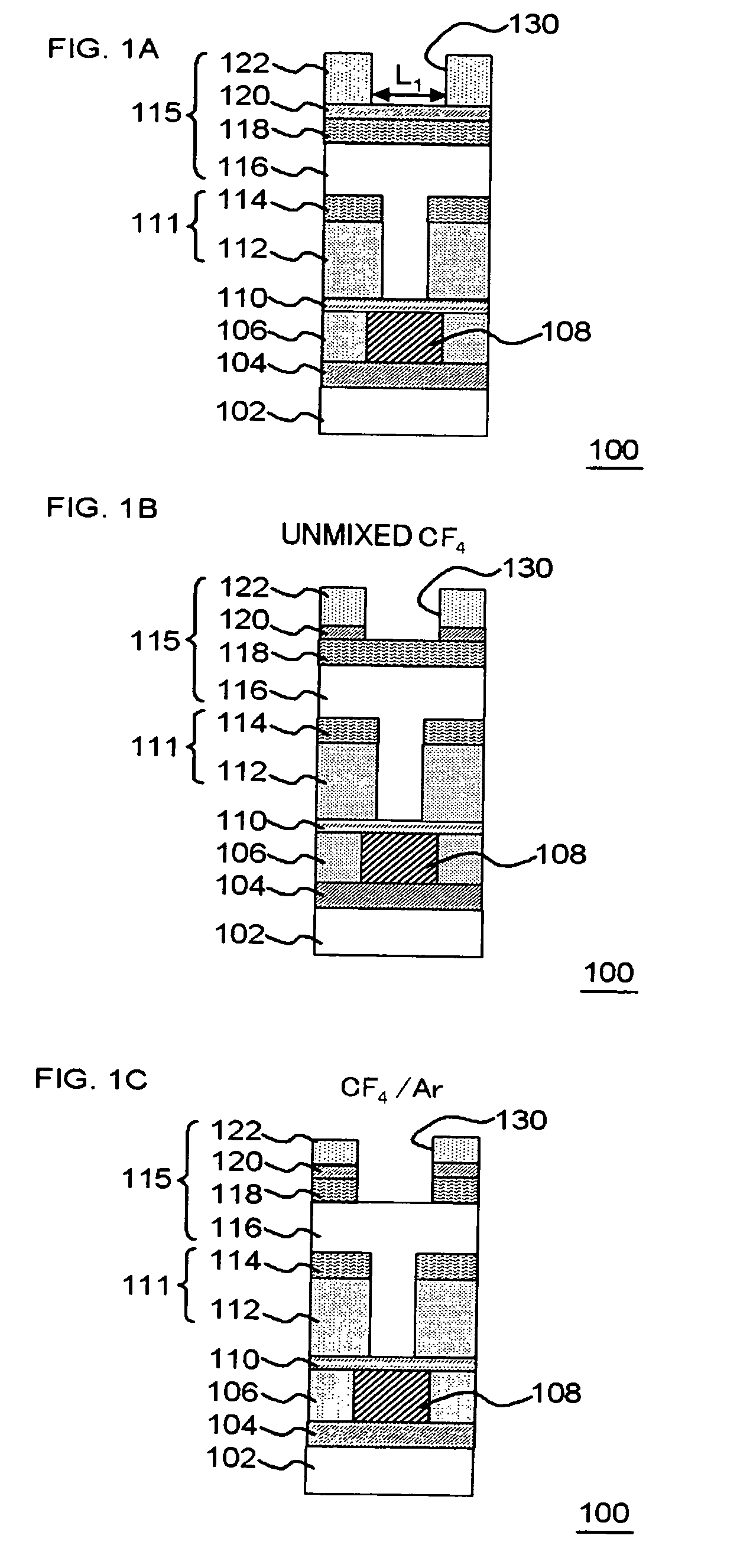
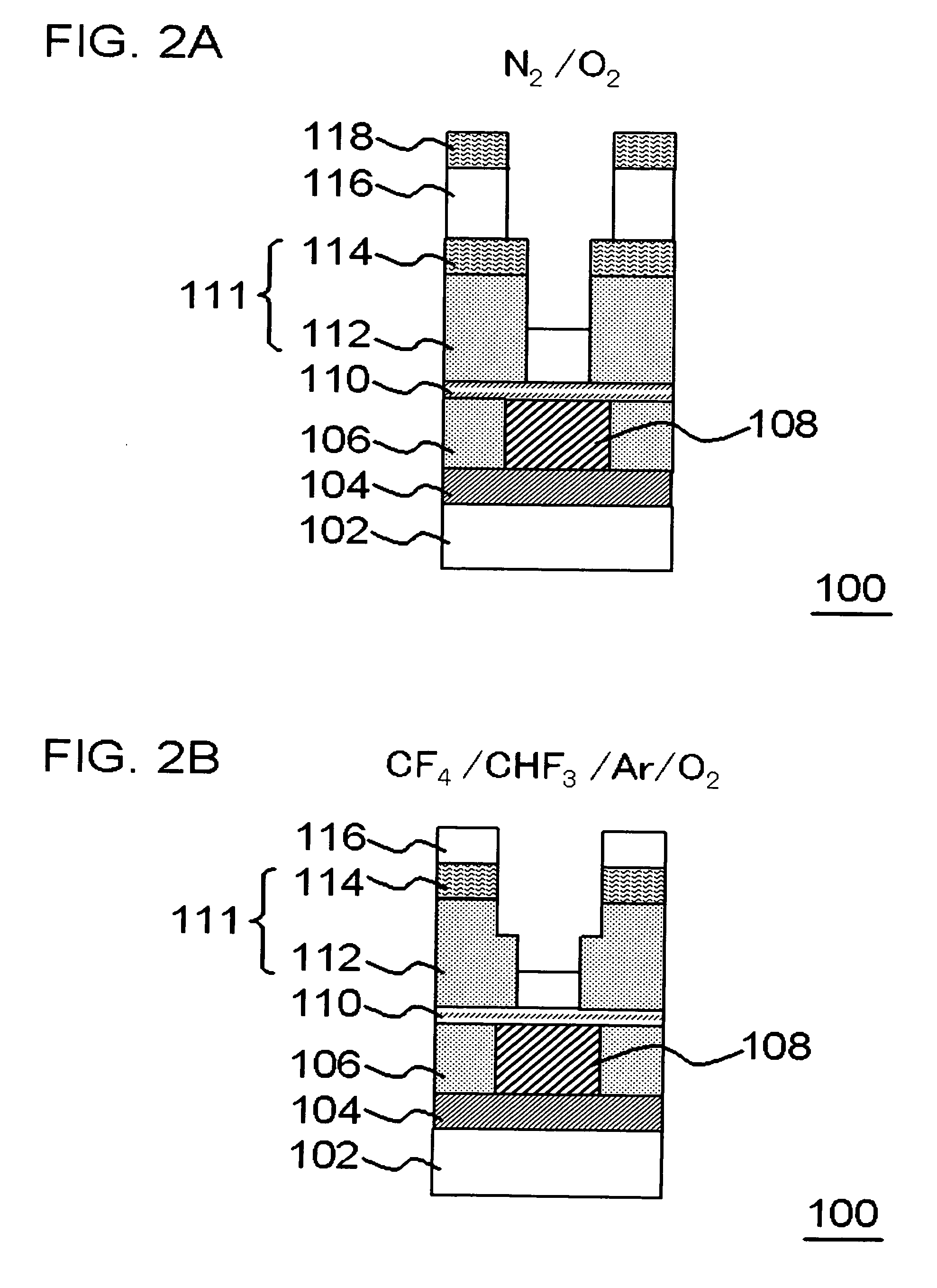
[0025]wherein in the etching the anti-reflective film in each of the forming the recess, a value of one etching condition correlative to a dimensional shift Δ(L2−L1), where L1 is a width of the opening in the upper resist film obtained in the forming the opening in the upper resist film and L2 is a width of a recess formed in the insulating film in the transferring the pattern, is varied with respect to the aperture ratio of an opening formed in the upper resist film so as to reduce the dimensional
Problems solved by technology
There has been a problem in that difference in the aperture ratio of pattern resulted in varied width of obtainable recesses, even if mask patterns having the same pattern width was used.
It takes a long time to achieve a steady vacuum state of the chamber again from the atmospheric pressure, and this means increase in so-called down time and serious degradation of operational efficiency of the apparatus.
However, the present inventors found out from their investigations that, in the process of forming the interconnect trench by the damascene proce
Method used
View moreImage
Smart ImageViewing Examples

Examples
 PUM
 Abstract
When a multi-layer structure is formed by forming the interconnect trenches or via holes having different patterns in a plurality of insulating films, an anti-reflective film and an upper resist film are stacked in this order over an insulating interlayer, and the anti-reflective film is etched through the upper resist film used as a mask, wherein the anti-reflective film is etched while varying a value of at least one etching condition correlative to Δ(L2−L1), expressing dimensional shift of width L2 of opening of the recess formed in the insulating film, with respect to width L1 of opening of the upper resist film, so as to reduce the dimensional shift Δ(L2−L1) as the aperture ratio of the opening to be formed in the upper resist film increases, depending on the aperture ratio.
Description
[0001]This application is based on Japanese patent application No. 2007-068584 the content of which is incorporated hereinto by reference.BACKGROUND[0002]1. Technical Field[0003]The present invention relates to a method of manufacturing a semiconductor device, and a control system.[0004]2. Related Art[0005]In recent semiconductor elements, delay in signal transmission in interconnects determines operation speed of elements. Delay constant of signal transmission in interconnects is expressed by a product of resistivity of interconnects and capacitance between the adjacent interconnects. Therefore, in view of increasing the operation speed of elements, there are growing trends of using low-dielectric-constant materials having dielectric constants smaller than that of conventional silicon oxide (SiO2) film as an insulating interlayer, and of using copper (Cu) having small resistivity as the interconnects.[0006]Multi-layer interconnects using copper as an interconnect material are forme...
Claims
Login to View More Application Information
Patent Timeline
 IPC IPC(8): H01L21/467H01L21/66
CPCH01L21/31116H01L21/76808H01L21/31144H01L21/31138
InventorNAMBU, HIDETAKA
OwnerRENESAS ELECTRONICS CORP